

emission energy
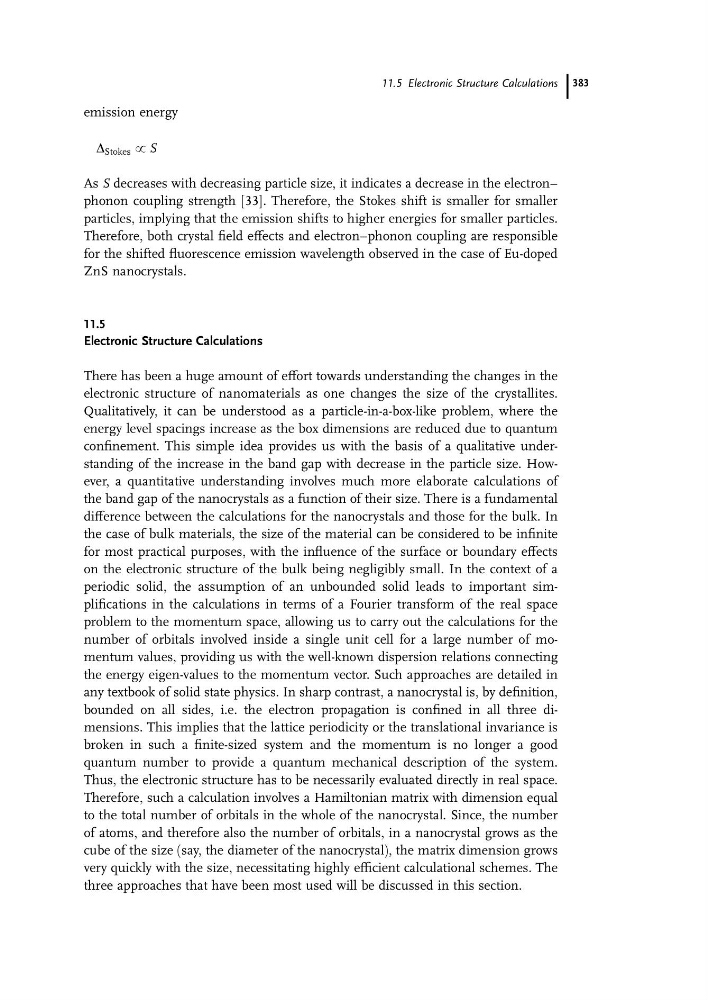
D Stokes z S
As S decreases with decreasing particle size, it indicates a decrease in the electron–
phonon coupling strength [33]. Therefore, the Stokes shift is smaller for smaller
particles, implying that the emission shifts to higher energies for smaller particles.
Therefore, both crystal field effects and electron–phonon coupling are responsible
for the shifted fluorescence emission wavelength observed in the case of Eu-doped
ZnS nanocrystals.
11.5
Electronic Structure Calculations
There has been a huge amount of effort towards understanding the changes in the
electronic structure of nanomaterials as one changes the size of the crystallites.
Qualitatively, it can be understood as a particle-in-a-box-like problem, where the
energy level spacings increase as the box dimensions are reduced due to quantum
confinement. This simple idea provides us with the basis of a qualitative understanding of the increase in the band gap with decrease in the particle size. However, a quantitative understanding involves much more elaborate calculations of
the band gap of the nanocrystals as a function of their size. There is a fundamental
difference between the calculations for the nanocrystals and those for the bulk. In
the case of bulk materials, the size of the material can be considered to be infinite
for most practical purposes, with the influence of the surface or boundary effects
on the electronic structure of the bulk being negligibly small. In the context of a
periodic solid, the assumption of an unbounded solid leads to important simplifications in the calculations in terms of a Fourier transform of the real space
problem to the momentum space, allowing us to carry out the calculations for the
number of orbitals involved inside a single unit cell for a large number of momentum values, providing us with the well-known dispersion relations connecting
the energy eigen-values to the momentum vector. Such approaches are detailed in
any textbook of solid state physics. In sharp contrast, a nanocrystal is, by definition,
bounded on all sides, i.e. the electron propagation is confined in all three dimensions. This implies that the lattice periodicity or the translational invariance is
broken in such a finite-sized system and the momentum is no longer a good
quantum number to provide a quantum mechanical description of the system.
Thus, the electronic structure has to be necessarily evaluated directly in real space.
Therefore, such a calculation involves a Hamiltonian matrix with dimension equal
to the total number of orbitals in the whole of the nanocrystal. Since, the number
of atoms, and therefore also the number of orbitals, in a nanocrystal grows as the
cube of the size (say, the diameter of the nanocrystal), the matrix dimension grows
very quickly with the size, necessitating highly efficient calculational schemes. The
three approaches that have been most used will be discussed in this section.
11.5 Electronic Structure Calculations 383
D Stokes z S
As S decreases with decreasing particle size, it indicates a decrease in the electron–
phonon coupling strength [33]. Therefore, the Stokes shift is smaller for smaller
particles, implying that the emission shifts to higher energies for smaller particles.
Therefore, both crystal field effects and electron–phonon coupling are responsible
for the shifted fluorescence emission wavelength observed in the case of Eu-doped
ZnS nanocrystals.
11.5
Electronic Structure Calculations
There has been a huge amount of effort towards understanding the changes in the
electronic structure of nanomaterials as one changes the size of the crystallites.
Qualitatively, it can be understood as a particle-in-a-box-like problem, where the
energy level spacings increase as the box dimensions are reduced due to quantum
confinement. This simple idea provides us with the basis of a qualitative understanding of the increase in the band gap with decrease in the particle size. However, a quantitative understanding involves much more elaborate calculations of
the band gap of the nanocrystals as a function of their size. There is a fundamental
difference between the calculations for the nanocrystals and those for the bulk. In
the case of bulk materials, the size of the material can be considered to be infinite
for most practical purposes, with the influence of the surface or boundary effects
on the electronic structure of the bulk being negligibly small. In the context of a
periodic solid, the assumption of an unbounded solid leads to important simplifications in the calculations in terms of a Fourier transform of the real space
problem to the momentum space, allowing us to carry out the calculations for the
number of orbitals involved inside a single unit cell for a large number of momentum values, providing us with the well-known dispersion relations connecting
the energy eigen-values to the momentum vector. Such approaches are detailed in
any textbook of solid state physics. In sharp contrast, a nanocrystal is, by definition,
bounded on all sides, i.e. the electron propagation is confined in all three dimensions. This implies that the lattice periodicity or the translational invariance is
broken in such a finite-sized system and the momentum is no longer a good
quantum number to provide a quantum mechanical description of the system.
Thus, the electronic structure has to be necessarily evaluated directly in real space.
Therefore, such a calculation involves a Hamiltonian matrix with dimension equal
to the total number of orbitals in the whole of the nanocrystal. Since, the number
of atoms, and therefore also the number of orbitals, in a nanocrystal grows as the
cube of the size (say, the diameter of the nanocrystal), the matrix dimension grows
very quickly with the size, necessitating highly efficient calculational schemes. The
three approaches that have been most used will be discussed in this section.
11.5 Electronic Structure Calculations 383