

electrons can occupy successively to de-excite to the ground state. In the absence of
strong phonon coupling, the electrons have to make a radiative transition that
often corresponds to energies close to the visible region of the electromagnetic
spectrum. This phenomenon, known as fluorescence, can occur in nanocrystals in
a variety of ways; for example, the electron–hole recombination can take place by
involving the electronic states at the band edge, surface, defect and other trap
states, or states on doped impurity atoms, giving rise to fluorescence at different
energies for the same material. We shall discuss these different routes in some
detail here.
Electrons can de-excite radiatively by making a transition from the bottom of the
conduction band (BCB) to the top of the valence band (TVB). This is known as
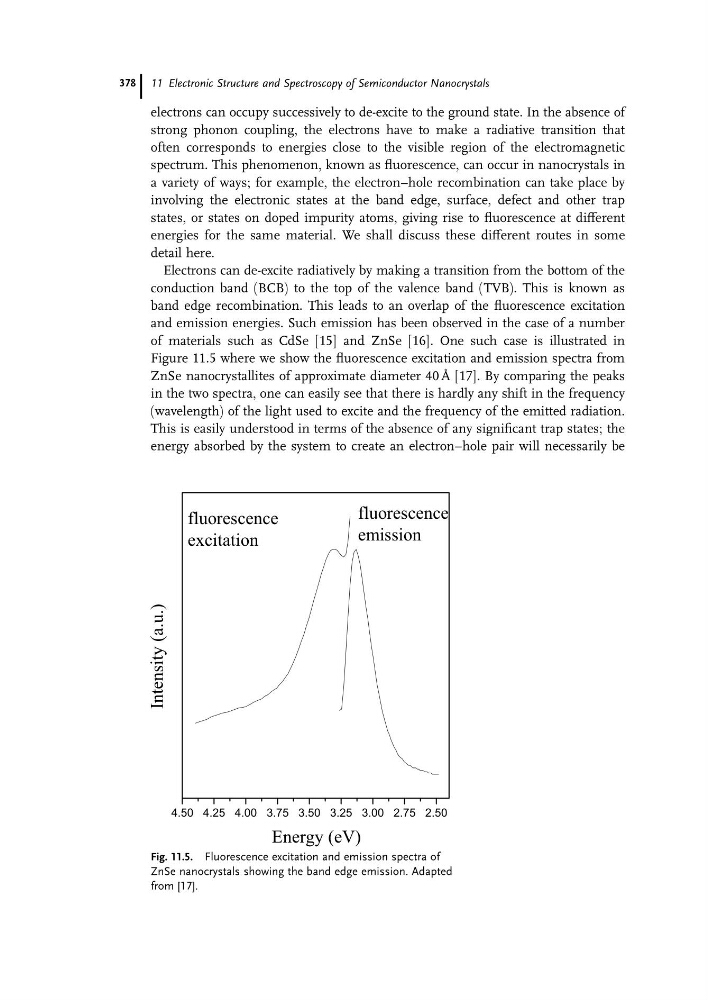
band edge recombination. This leads to an overlap of the fluorescence excitation
and emission energies. Such emission has been observed in the case of a number
of materials such as CdSe [15] and ZnSe [16]. One such case is illustrated in
Figure 11.5 where we show the fluorescence excitation and emission spectra from
ZnSe nanocrystallites of approximate diameter 40 A ˚ [17]. By comparing the peaks
in the two spectra, one can easily see that there is hardly any shift in the frequency
(wavelength) of the light used to excite and the frequency of the emitted radiation.
This is easily understood in terms of the absence of any significant trap states; the
energy absorbed by the system to create an electron–hole pair will necessarily be
4.50 4.25 4.00 3.75 3.50 3.25 3.00 2.75 2.50
fluorescence
excitation
fluorescence
emission
Intensity (a.u.)
Energy (eV)
Fig. 11.5. Fluorescence excitation and emission spectra of
ZnSe nanocrystals showing the band edge emission. Adapted
from [17].
11 Electronic Structure and Spectroscopy of Semiconductor Nanocrystals
378
strong phonon coupling, the electrons have to make a radiative transition that
often corresponds to energies close to the visible region of the electromagnetic
spectrum. This phenomenon, known as fluorescence, can occur in nanocrystals in
a variety of ways; for example, the electron–hole recombination can take place by
involving the electronic states at the band edge, surface, defect and other trap
states, or states on doped impurity atoms, giving rise to fluorescence at different
energies for the same material. We shall discuss these different routes in some
detail here.
Electrons can de-excite radiatively by making a transition from the bottom of the
conduction band (BCB) to the top of the valence band (TVB). This is known as
band edge recombination. This leads to an overlap of the fluorescence excitation
and emission energies. Such emission has been observed in the case of a number
of materials such as CdSe [15] and ZnSe [16]. One such case is illustrated in
Figure 11.5 where we show the fluorescence excitation and emission spectra from
ZnSe nanocrystallites of approximate diameter 40 A ˚ [17]. By comparing the peaks
in the two spectra, one can easily see that there is hardly any shift in the frequency
(wavelength) of the light used to excite and the frequency of the emitted radiation.
This is easily understood in terms of the absence of any significant trap states; the
energy absorbed by the system to create an electron–hole pair will necessarily be
4.50 4.25 4.00 3.75 3.50 3.25 3.00 2.75 2.50
fluorescence
excitation
fluorescence
emission
Intensity (a.u.)
Energy (eV)
Fig. 11.5. Fluorescence excitation and emission spectra of
ZnSe nanocrystals showing the band edge emission. Adapted
from [17].
11 Electronic Structure and Spectroscopy of Semiconductor Nanocrystals
378