

equal to the energy emitted, when the electron and the hole recombine without the
loss of any energy prior to the emission.
The presence of unquenched dangling orbitals at the surface or any defect states
in the bulk, provide traps for the excited electrons and the holes prior to their recombination. These orbitals have their energies in the band gap region, as shall be
discussed in greater detail in Section 11.5. Therefore, an electron excited to the
conduction band can transfer itself non-radiatively to one of these surface or defect
states before making a radiative transition to a lower energy state; likewise, a hole
excited in the valence band can move into the defect states depending upon the
donor/acceptor character of the defect states. The net result of such non-radiative
transfers of electrons and holes to lower energy states prior to radiative recombination is that the emission occurs at energies much lower than the band gap energy of the nanocrystals, in contrast to the band edge recombination considered
earlier. This is often referred to as the red-shifted emission in nanocrystals [18].
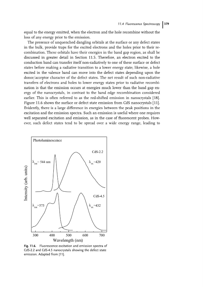
Figure 11.6 shows the surface or defect state emission from CdS nanocrystals [11].
Evidently, there is a large difference in energies between the peak positions in the
excitation and the emission spectra. Such an emission is useful where one requires
well separated excitation and emission, as in the case of fluorescent probes. However, such defect states tend to be spread over a wide energy range, leading to
300
400
500
600
700
ex
=420
CdS-2.2
Intensity (arb. units)
em
=575
em
= 544 nm
ex
=432
CdS-4.5
Wavelength (nm)
Photoluminescence
λ
λ
λ
λ
Fig. 11.6. Fluorescence excitation and emission spectra of
CdS-2.2 and CdS-4.5 nanocrystals showing the defect state
emission. Adapted from [11].
11.4 Fluorescence Spectroscopy 379
loss of any energy prior to the emission.
The presence of unquenched dangling orbitals at the surface or any defect states
in the bulk, provide traps for the excited electrons and the holes prior to their recombination. These orbitals have their energies in the band gap region, as shall be
discussed in greater detail in Section 11.5. Therefore, an electron excited to the
conduction band can transfer itself non-radiatively to one of these surface or defect
states before making a radiative transition to a lower energy state; likewise, a hole
excited in the valence band can move into the defect states depending upon the
donor/acceptor character of the defect states. The net result of such non-radiative
transfers of electrons and holes to lower energy states prior to radiative recombination is that the emission occurs at energies much lower than the band gap energy of the nanocrystals, in contrast to the band edge recombination considered
earlier. This is often referred to as the red-shifted emission in nanocrystals [18].
Figure 11.6 shows the surface or defect state emission from CdS nanocrystals [11].
Evidently, there is a large difference in energies between the peak positions in the
excitation and the emission spectra. Such an emission is useful where one requires
well separated excitation and emission, as in the case of fluorescent probes. However, such defect states tend to be spread over a wide energy range, leading to
300
400
500
600
700
ex
=420
CdS-2.2
Intensity (arb. units)
em
=575
em
= 544 nm
ex
=432
CdS-4.5
Wavelength (nm)
Photoluminescence
λ
λ
λ
λ
Fig. 11.6. Fluorescence excitation and emission spectra of
CdS-2.2 and CdS-4.5 nanocrystals showing the defect state
emission. Adapted from [11].
11.4 Fluorescence Spectroscopy 379