

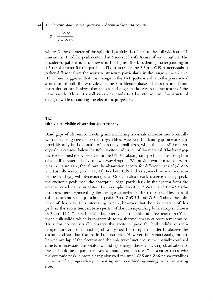
D ¼
4
3
0:9l
B cos y
where D, the diameter of the spherical particles is related to the full-width-at-halfmaximum, B, of the peak centered at y recorded with X-rays of wavelength l. The
broadened pattern is also shown in the figure; the broadening corresponding to
4.5 nm diameter for the particles. The pattern for the 2.2 nm CdS nanocrystals is
rather different from the wurtzite structure particularly in the range 2y ¼ 45–55
.
It has been suggested that this change in the XRD pattern is due to the presence of
a mixture of both the wurtzite and the zinc-blende phases. This structural transformation at small sizes also causes a change in the electronic structure of the
nanocrystals. Thus, at small sizes one needs to take into account the structural
changes while discussing the electronic properties.
11.3
Ultraviolet–Visible Absorption Spectroscopy
Band gaps of all semiconducting and insulating materials increase monotonically
with decreasing size of the nanocrystallites. However, the band gap increases appreciably only in the domain of extremely small sizes, when the size of the nanocrystals is reduced below the Bohr exciton radius, a B of the material. The band gap
increase is most easily observed in the UV–Vis absorption spectra as the absorption
edge shifts systematically to lower wavelengths. We provide two illustrative examples in Figure 11.2, that shows the absorption spectra for different sizes of (a) ZnS
and (b) CdS nanocrystals [11, 12]. For both CdS and ZnS, we observe an increase
in the band gap with decreasing size. One can also clearly observe a sharp peak,
the excitonic peak, near the absorption edge, particularly in the spectra from the
smaller sized nanocrystallites. For example ZnS-1.8, ZnS-2.5 and CdS-2.2 (the
numbers here representing the average diameter of the nanocrystallites in nm)
exhibit extremely sharp excitonic peaks. Even ZnS-3.5 and CdS-4.5 show the existence of this peak. It is interesting to note, however, that there is no trace of this
peak in the room temperature spectra of the corresponding bulk samples shown
in Figure 11.2. The exciton binding energy is of the order of a few tens of meV for
these bulk solids, which is comparable to the thermal energy at room temperature.
Thus, we do not usually observe the excitonic peak for bulk solids at room
temperature and one must significantly cool the sample in order to observe the
excitonic absorption feature in bulk samples. However, for nanocrystals, the enhanced overlap of the electron and the hole wavefunctions in the spatially confined
structure increases the excitonic binding energy, thereby making observation of
the excitonic peak possible, even at room temperature. This also explains why
the excitonic peak is more clearly observed for small CdS and ZnS nanocrystallites
in terms of a progressively increasing excitonic binding energy with decreasing
size.
11 Electronic Structure and Spectroscopy of Semiconductor Nanocrystals
374
4
3
0:9l
B cos y
where D, the diameter of the spherical particles is related to the full-width-at-halfmaximum, B, of the peak centered at y recorded with X-rays of wavelength l. The
broadened pattern is also shown in the figure; the broadening corresponding to
4.5 nm diameter for the particles. The pattern for the 2.2 nm CdS nanocrystals is
rather different from the wurtzite structure particularly in the range 2y ¼ 45–55
.
It has been suggested that this change in the XRD pattern is due to the presence of
a mixture of both the wurtzite and the zinc-blende phases. This structural transformation at small sizes also causes a change in the electronic structure of the
nanocrystals. Thus, at small sizes one needs to take into account the structural
changes while discussing the electronic properties.
11.3
Ultraviolet–Visible Absorption Spectroscopy
Band gaps of all semiconducting and insulating materials increase monotonically
with decreasing size of the nanocrystallites. However, the band gap increases appreciably only in the domain of extremely small sizes, when the size of the nanocrystals is reduced below the Bohr exciton radius, a B of the material. The band gap
increase is most easily observed in the UV–Vis absorption spectra as the absorption
edge shifts systematically to lower wavelengths. We provide two illustrative examples in Figure 11.2, that shows the absorption spectra for different sizes of (a) ZnS
and (b) CdS nanocrystals [11, 12]. For both CdS and ZnS, we observe an increase
in the band gap with decreasing size. One can also clearly observe a sharp peak,
the excitonic peak, near the absorption edge, particularly in the spectra from the
smaller sized nanocrystallites. For example ZnS-1.8, ZnS-2.5 and CdS-2.2 (the
numbers here representing the average diameter of the nanocrystallites in nm)
exhibit extremely sharp excitonic peaks. Even ZnS-3.5 and CdS-4.5 show the existence of this peak. It is interesting to note, however, that there is no trace of this
peak in the room temperature spectra of the corresponding bulk samples shown
in Figure 11.2. The exciton binding energy is of the order of a few tens of meV for
these bulk solids, which is comparable to the thermal energy at room temperature.
Thus, we do not usually observe the excitonic peak for bulk solids at room
temperature and one must significantly cool the sample in order to observe the
excitonic absorption feature in bulk samples. However, for nanocrystals, the enhanced overlap of the electron and the hole wavefunctions in the spatially confined
structure increases the excitonic binding energy, thereby making observation of
the excitonic peak possible, even at room temperature. This also explains why
the excitonic peak is more clearly observed for small CdS and ZnS nanocrystallites
in terms of a progressively increasing excitonic binding energy with decreasing
size.
11 Electronic Structure and Spectroscopy of Semiconductor Nanocrystals
374