

[112] and [110]. We thus speculate that the zigzag shape originates from a periodic
transition between two growth directions (which is 30 between [112] and [110] and
35 between [110] and [111]).
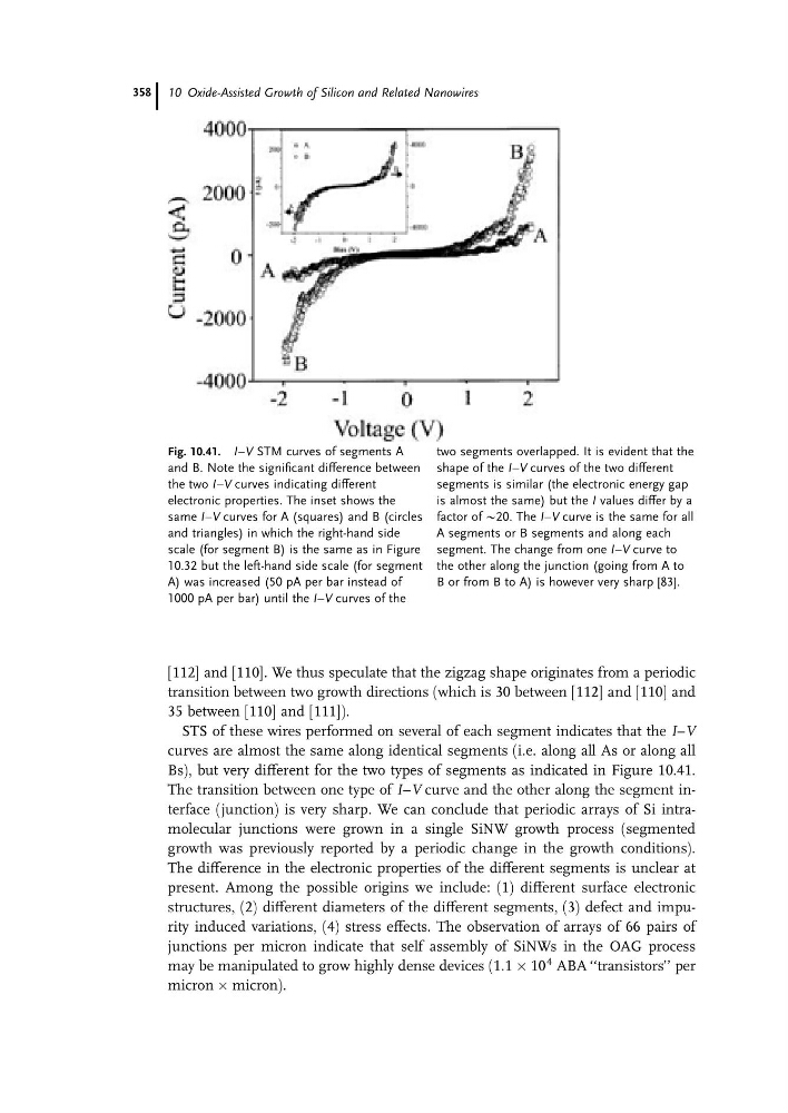
STS of these wires performed on several of each segment indicates that the I–V
curves are almost the same along identical segments (i.e. along all As or along all
Bs), but very different for the two types of segments as indicated in Figure 10.41.
The transition between one type of I–V curve and the other along the segment interface (junction) is very sharp. We can conclude that periodic arrays of Si intramolecular junctions were grown in a single SiNW growth process (segmented
growth was previously reported by a periodic change in the growth conditions).
The difference in the electronic properties of the different segments is unclear at
present. Among the possible origins we include: (1) different surface electronic
structures, (2) different diameters of the different segments, (3) defect and impurity induced variations, (4) stress effects. The observation of arrays of 66 pairs of
junctions per micron indicate that self assembly of SiNWs in the OAG process
may be manipulated to grow highly dense devices (1:1 Â 10
4 ABA ‘‘transistors’’ per
micron  micron).
Fig. 10.41. I–V STM curves of segments A
and B. Note the significant difference between
the two I–V curves indicating different
electronic properties. The inset shows the
same I–V curves for A (squares) and B (circles
and triangles) in which the right-hand side
scale (for segment B) is the same as in Figure
10.32 but the left-hand side scale (for segment
A) was increased (50 pA per bar instead of
1000 pA per bar) until the I–V curves of the
two segments overlapped. It is evident that the
shape of the I–V curves of the two different
segments is similar (the electronic energy gap
is almost the same) but the I values differ by a
factor of @20. The I–V curve is the same for all
A segments or B segments and along each
segment. The change from one I–V curve to
the other along the junction (going from A to
B or from B to A) is however very sharp [83].
10 Oxide-Assisted Growth of Silicon and Related Nanowires
358
transition between two growth directions (which is 30 between [112] and [110] and
35 between [110] and [111]).
STS of these wires performed on several of each segment indicates that the I–V
curves are almost the same along identical segments (i.e. along all As or along all
Bs), but very different for the two types of segments as indicated in Figure 10.41.
The transition between one type of I–V curve and the other along the segment interface (junction) is very sharp. We can conclude that periodic arrays of Si intramolecular junctions were grown in a single SiNW growth process (segmented
growth was previously reported by a periodic change in the growth conditions).
The difference in the electronic properties of the different segments is unclear at
present. Among the possible origins we include: (1) different surface electronic
structures, (2) different diameters of the different segments, (3) defect and impurity induced variations, (4) stress effects. The observation of arrays of 66 pairs of
junctions per micron indicate that self assembly of SiNWs in the OAG process
may be manipulated to grow highly dense devices (1:1 Â 10
4 ABA ‘‘transistors’’ per
micron  micron).
Fig. 10.41. I–V STM curves of segments A
and B. Note the significant difference between
the two I–V curves indicating different
electronic properties. The inset shows the
same I–V curves for A (squares) and B (circles
and triangles) in which the right-hand side
scale (for segment B) is the same as in Figure
10.32 but the left-hand side scale (for segment
A) was increased (50 pA per bar instead of
1000 pA per bar) until the I–V curves of the
two segments overlapped. It is evident that the
shape of the I–V curves of the two different
segments is similar (the electronic energy gap
is almost the same) but the I values differ by a
factor of @20. The I–V curve is the same for all
A segments or B segments and along each
segment. The change from one I–V curve to
the other along the junction (going from A to
B or from B to A) is however very sharp [83].
10 Oxide-Assisted Growth of Silicon and Related Nanowires
358