

UHV STM system. Among the less abundant forms of SiNWs, @1% have a zigzag
shape, composed of many bends or junctions.
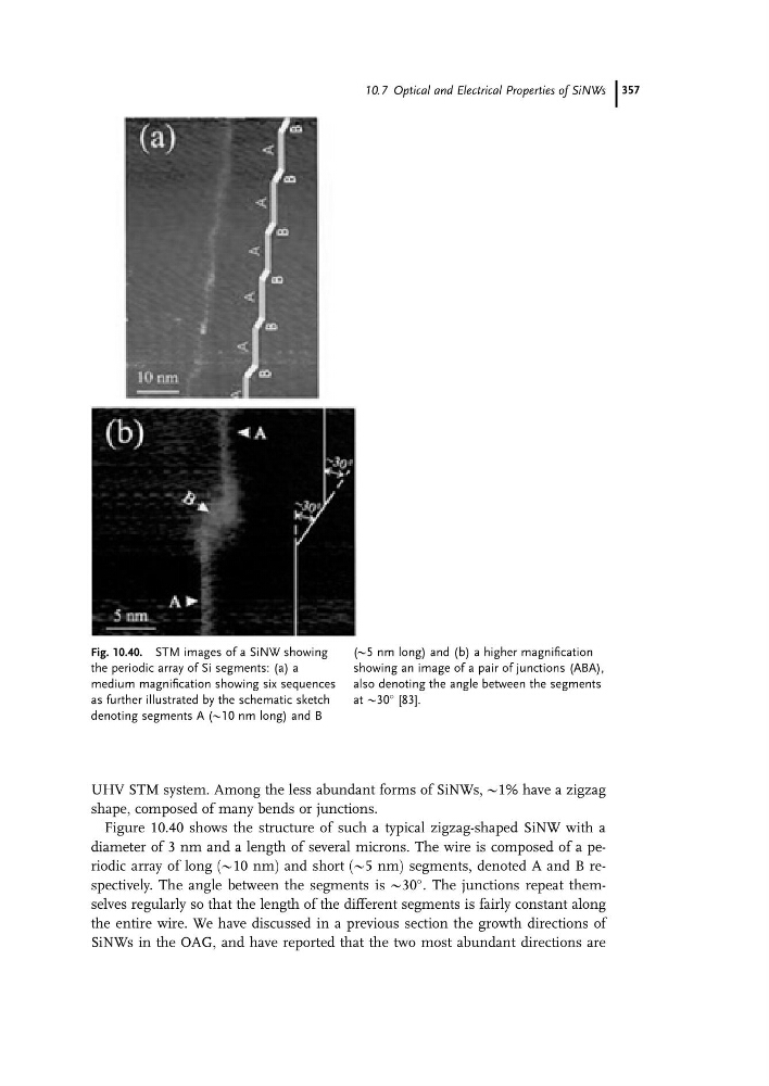
Figure 10.40 shows the structure of such a typical zigzag-shaped SiNW with a
diameter of 3 nm and a length of several microns. The wire is composed of a periodic array of long (@10 nm) and short (@5 nm) segments, denoted A and B respectively. The angle between the segments is @30
. The junctions repeat themselves regularly so that the length of the different segments is fairly constant along
the entire wire. We have discussed in a previous section the growth directions of
SiNWs in the OAG, and have reported that the two most abundant directions are
Fig. 10.40. STM images of a SiNW showing
the periodic array of Si segments: (a) a
medium magnification showing six sequences
as further illustrated by the schematic sketch
denoting segments A (@10 nm long) and B
(@5 nm long) and (b) a higher magnification
showing an image of a pair of junctions (ABA),
also denoting the angle between the segments
at @30
[83].
10.7 Optical and Electrical Properties of SiNWs 357
shape, composed of many bends or junctions.
Figure 10.40 shows the structure of such a typical zigzag-shaped SiNW with a
diameter of 3 nm and a length of several microns. The wire is composed of a periodic array of long (@10 nm) and short (@5 nm) segments, denoted A and B respectively. The angle between the segments is @30
. The junctions repeat themselves regularly so that the length of the different segments is fairly constant along
the entire wire. We have discussed in a previous section the growth directions of
SiNWs in the OAG, and have reported that the two most abundant directions are
Fig. 10.40. STM images of a SiNW showing
the periodic array of Si segments: (a) a
medium magnification showing six sequences
as further illustrated by the schematic sketch
denoting segments A (@10 nm long) and B
(@5 nm long) and (b) a higher magnification
showing an image of a pair of junctions (ABA),
also denoting the angle between the segments
at @30
[83].
10.7 Optical and Electrical Properties of SiNWs 357