

the chain are clearly revealed as evenly spaced bright dots of uniform size. Figure
10.39(b) shows a typical straight nanowire, the diameter of which is about 35 nm.
Occasionally, sharp images of SiNW of ca. 40 nm in diameter, as shown in Figure
10.39(c), were obtained via air STM. The image reveals clearly resolved rectangular domains of several nanometers in size. These domains are associated with
B-induced reconstruction of the silicon surface, and the clear images were
made possible by B-enhanced conductivity.
STS measurements have also been performed on the undoped and B-doped
SiNWs shown in Figure 10.39. The I–V and the corresponding differentiated dI/dV
curves of the nanowires reveal several features. First, while the curves for the two
B-doped nanowires with different morphologies are quite similar, they are distinctly different from that for the undoped wire. This is because, as far as tunneling from a STM probe is concerned, the particle in the nanochain is the same as
any point on a nanowire with a similar doping concentration and oxide sheath.
Second, the steeper rise in the I–V curves and the higher values of dI/dV for the
B-doped SiNWs are consistent with the expected B-induced conductivity enhancement. As dI/dV values can be regarded as a measure of local density of states
(LDOS), the low value between À1 to þ1 V in the dI/dV curve of the undoped wire
indicates relatively little LDOS within the gap, while the higher dI/dV in the same
region of the doped wires is in accord with the presence of the B dopants. The
minima of the curves are at 0.3 V, indicating that the Fermi level in the B-doped
SiNWs lies 0.3 eV closer to the valence band relative to the undoped wire. The
position of the Fermi level corresponds to a hole carrier concentration of 1:5 Â
10
15 cm
À3 in the boron-doped nanowires.
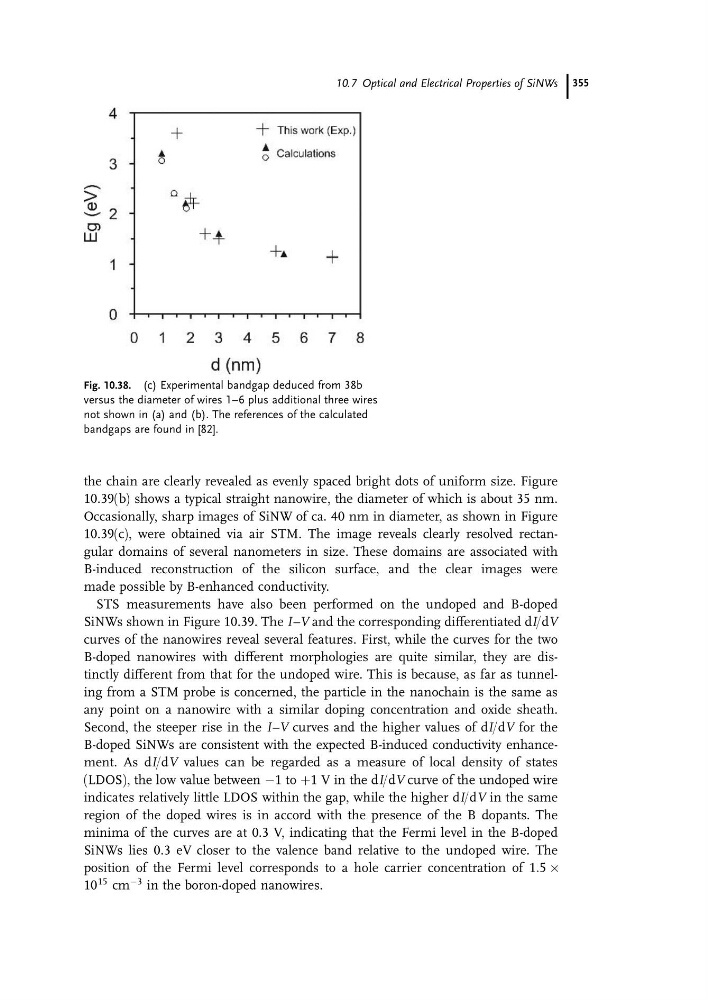
Fig. 10.38. (c) Experimental bandgap deduced from 38b
versus the diameter of wires 1–6 plus additional three wires
not shown in (a) and (b). The references of the calculated
bandgaps are found in [82].
10.7 Optical and Electrical Properties of SiNWs 355
10.39(b) shows a typical straight nanowire, the diameter of which is about 35 nm.
Occasionally, sharp images of SiNW of ca. 40 nm in diameter, as shown in Figure
10.39(c), were obtained via air STM. The image reveals clearly resolved rectangular domains of several nanometers in size. These domains are associated with
B-induced reconstruction of the silicon surface, and the clear images were
made possible by B-enhanced conductivity.
STS measurements have also been performed on the undoped and B-doped
SiNWs shown in Figure 10.39. The I–V and the corresponding differentiated dI/dV
curves of the nanowires reveal several features. First, while the curves for the two
B-doped nanowires with different morphologies are quite similar, they are distinctly different from that for the undoped wire. This is because, as far as tunneling from a STM probe is concerned, the particle in the nanochain is the same as
any point on a nanowire with a similar doping concentration and oxide sheath.
Second, the steeper rise in the I–V curves and the higher values of dI/dV for the
B-doped SiNWs are consistent with the expected B-induced conductivity enhancement. As dI/dV values can be regarded as a measure of local density of states
(LDOS), the low value between À1 to þ1 V in the dI/dV curve of the undoped wire
indicates relatively little LDOS within the gap, while the higher dI/dV in the same
region of the doped wires is in accord with the presence of the B dopants. The
minima of the curves are at 0.3 V, indicating that the Fermi level in the B-doped
SiNWs lies 0.3 eV closer to the valence band relative to the undoped wire. The
position of the Fermi level corresponds to a hole carrier concentration of 1:5 Â
10
15 cm
À3 in the boron-doped nanowires.
Fig. 10.38. (c) Experimental bandgap deduced from 38b
versus the diameter of wires 1–6 plus additional three wires
not shown in (a) and (b). The references of the calculated
bandgaps are found in [82].
10.7 Optical and Electrical Properties of SiNWs 355