

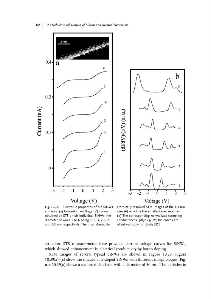
struction. STS measurements have provided current–voltage curves for SiNWs,
which showed enhancement in electrical conductivity by boron doping.
STM images of several typical SiNWs are shown in Figure 10.39. Figure
10.39(a)–(c) show the images of B-doped SiNWs with different morphologies. Figure 10.39(a) shows a nanoparticle chain with a diameter of 30 nm. The particles in
Fig. 10.38. Electronic properties of the SiNWs
surfaces: (a) Current (I)–voltage (V ) curves
obtained by STS on six individual SiNWs; the
diameter of wires 1 to 6 being 7, 5, 3, 2.5, 2,
and 1.3 nm respectively. The inset shows the
atomically resolved STM images of the 1.3 nm
wire (6) which is the smallest ever reported.
(b) The corresponding normalized tunneling
conductances, (dI/dV )/I/V; the curves are
offset vertically for clarity [82].
10 Oxide-Assisted Growth of Silicon and Related Nanowires
354
which showed enhancement in electrical conductivity by boron doping.
STM images of several typical SiNWs are shown in Figure 10.39. Figure
10.39(a)–(c) show the images of B-doped SiNWs with different morphologies. Figure 10.39(a) shows a nanoparticle chain with a diameter of 30 nm. The particles in
Fig. 10.38. Electronic properties of the SiNWs
surfaces: (a) Current (I)–voltage (V ) curves
obtained by STS on six individual SiNWs; the
diameter of wires 1 to 6 being 7, 5, 3, 2.5, 2,
and 1.3 nm respectively. The inset shows the
atomically resolved STM images of the 1.3 nm
wire (6) which is the smallest ever reported.
(b) The corresponding normalized tunneling
conductances, (dI/dV )/I/V; the curves are
offset vertically for clarity [82].
10 Oxide-Assisted Growth of Silicon and Related Nanowires
354