

electronic energy bandgaps increase with decreasing SiNW diameter from 1.1 eV
for 7 nm to 3.5 eV for 1.3 nm in accord with previous theoretical predictions (Figure 10.38(c)), demonstrating a quantum size effect [82].
STM and STS measurements have been also performed on B-doped and undoped SiNWS [45] produced by OAG [23, 80]. The as-grown sample consisted primarily of SiNWs and nanoparticle chains coated with an oxide sheath. Samples
for STM and STS measurements were prepared by dispersing the SiNWs into a
suspension, which was then spin-coated onto highly oriented pyrolytic graphite
(HOPG) substrates. The presence of nanoparticle chains and nanowires in the Bdoped SiNWs sample was observed. Clear and regular nanoscale domains were
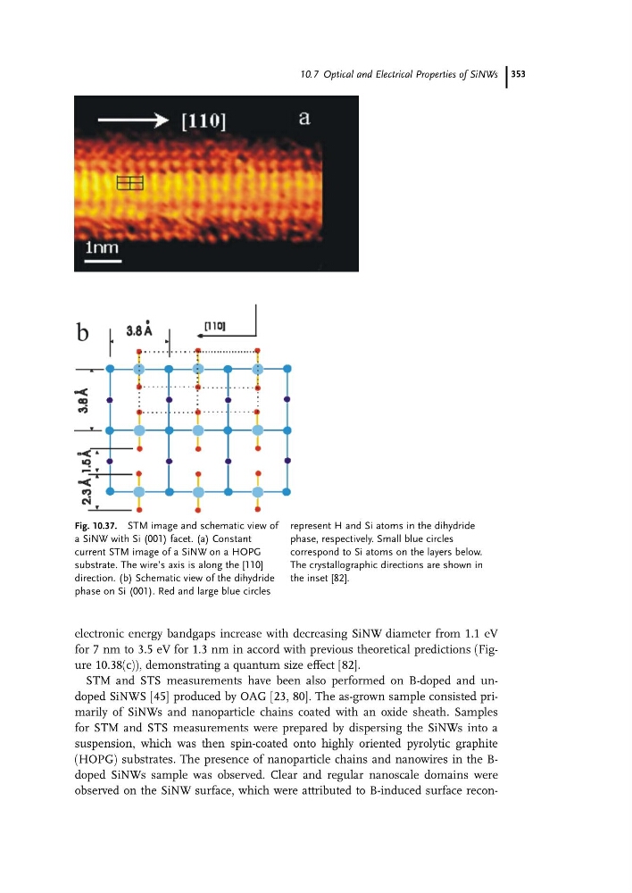
observed on the SiNW surface, which were attributed to B-induced surface reconFig. 10.37. STM image and schematic view of
a SiNW with Si (001) facet. (a) Constant
current STM image of a SiNW on a HOPG
substrate. The wire’s axis is along the [110]
direction. (b) Schematic view of the dihydride
phase on Si (001). Red and large blue circles
represent H and Si atoms in the dihydride
phase, respectively. Small blue circles
correspond to Si atoms on the layers below.
The crystallographic directions are shown in
the inset [82].
10.7 Optical and Electrical Properties of SiNWs 353
for 7 nm to 3.5 eV for 1.3 nm in accord with previous theoretical predictions (Figure 10.38(c)), demonstrating a quantum size effect [82].
STM and STS measurements have been also performed on B-doped and undoped SiNWS [45] produced by OAG [23, 80]. The as-grown sample consisted primarily of SiNWs and nanoparticle chains coated with an oxide sheath. Samples
for STM and STS measurements were prepared by dispersing the SiNWs into a
suspension, which was then spin-coated onto highly oriented pyrolytic graphite
(HOPG) substrates. The presence of nanoparticle chains and nanowires in the Bdoped SiNWs sample was observed. Clear and regular nanoscale domains were
observed on the SiNW surface, which were attributed to B-induced surface reconFig. 10.37. STM image and schematic view of
a SiNW with Si (001) facet. (a) Constant
current STM image of a SiNW on a HOPG
substrate. The wire’s axis is along the [110]
direction. (b) Schematic view of the dihydride
phase on Si (001). Red and large blue circles
represent H and Si atoms in the dihydride
phase, respectively. Small blue circles
correspond to Si atoms on the layers below.
The crystallographic directions are shown in
the inset [82].
10.7 Optical and Electrical Properties of SiNWs 353