

where the oxide serves as the reactant) induced nucleation and growth of a nanowire embedded in an oxide sheath follow [22–27, 73]. The chemical reaction induced nucleation and growth of nanowires differentiates the OAG from the conventional metal catalyst VLS growth. The oxide-assisted nanowire growth process
is free of metal catalysts thus enabling the formation of pure nanowires.
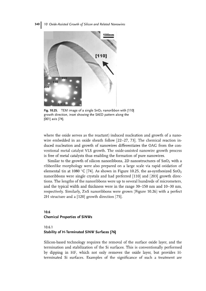
Similar to the growth of silicon nanoribbons, 2D nanostructures of SnO 2 with a
ribbonlike morphology were also prepared on a large scale via rapid oxidation of
elemental tin at 1080
C [74]. As shown in Figure 10.25, the as-synthesized SnO 2
nanoribbons were single crystals and had preferred [110] and [203] growth directions. The lengths of the nanoribbons were up to several hundreds of micrometers,
and the typical width and thickness were in the range 30–150 nm and 10–30 nm,
respectively. Similarly, ZnS nanoribbons were grown (Figure 10.26) with a perfect
2H structure and a [120] growth direction [75].
10.6
Chemical Properties of SiNWs
10.6.1
Stability of H-Terminated SiNW Surfaces [76]
Silicon-based technology requires the removal of the surface oxide layer, and the
termination and stabilization of the Si surfaces. This is conventionally performed
by dipping in HF, which not only removes the oxide layer, but provides Hterminated Si surfaces. Examples of the significance of such a treatment are
Fig. 10.25. TEM image of a single SnO 2 nanoribbon with [110]
growth direction, inset showing the SAED pattern along the
[001] axis [74].
10 Oxide-Assisted Growth of Silicon and Related Nanowires
340
is free of metal catalysts thus enabling the formation of pure nanowires.
Similar to the growth of silicon nanoribbons, 2D nanostructures of SnO 2 with a
ribbonlike morphology were also prepared on a large scale via rapid oxidation of
elemental tin at 1080
C [74]. As shown in Figure 10.25, the as-synthesized SnO 2
nanoribbons were single crystals and had preferred [110] and [203] growth directions. The lengths of the nanoribbons were up to several hundreds of micrometers,
and the typical width and thickness were in the range 30–150 nm and 10–30 nm,
respectively. Similarly, ZnS nanoribbons were grown (Figure 10.26) with a perfect
2H structure and a [120] growth direction [75].
10.6
Chemical Properties of SiNWs
10.6.1
Stability of H-Terminated SiNW Surfaces [76]
Silicon-based technology requires the removal of the surface oxide layer, and the
termination and stabilization of the Si surfaces. This is conventionally performed
by dipping in HF, which not only removes the oxide layer, but provides Hterminated Si surfaces. Examples of the significance of such a treatment are
Fig. 10.25. TEM image of a single SnO 2 nanoribbon with [110]
growth direction, inset showing the SAED pattern along the
[001] axis [74].
10 Oxide-Assisted Growth of Silicon and Related Nanowires
340