

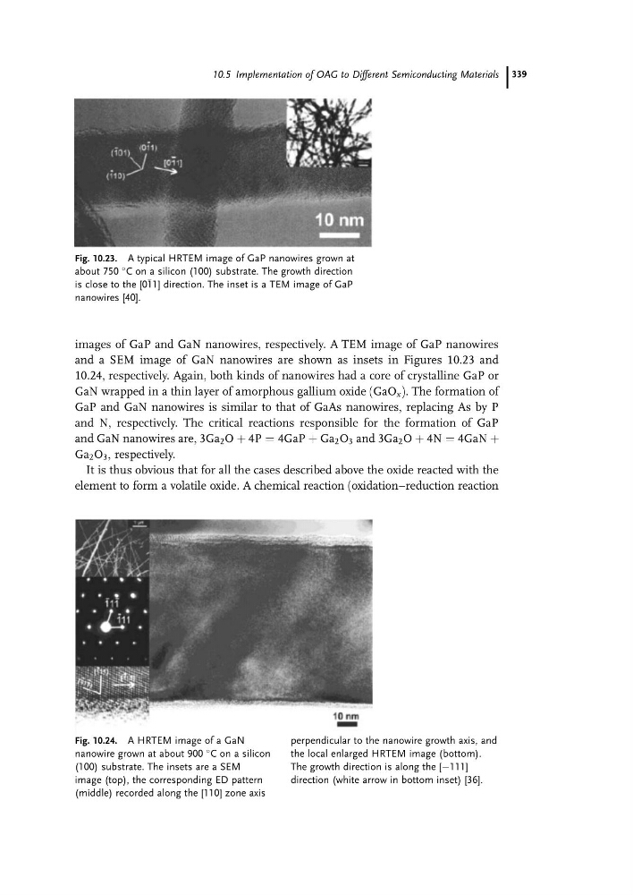
images of GaP and GaN nanowires, respectively. A TEM image of GaP nanowires
and a SEM image of GaN nanowires are shown as insets in Figures 10.23 and
10.24, respectively. Again, both kinds of nanowires had a core of crystalline GaP or
GaN wrapped in a thin layer of amorphous gallium oxide (GaO x ). The formation of
GaP and GaN nanowires is similar to that of GaAs nanowires, replacing As by P
and N, respectively. The critical reactions responsible for the formation of GaP
and GaN nanowires are, 3Ga 2 O þ 4P ¼ 4GaP þ Ga 2 O 3 and 3Ga 2 O þ 4N ¼ 4GaN þ
Ga 2 O 3 , respectively.
It is thus obvious that for all the cases described above the oxide reacted with the
element to form a volatile oxide. A chemical reaction (oxidation–reduction reaction
Fig. 10.23. A typical HRTEM image of GaP nanowires grown at
about 750
C on a silicon (100) substrate. The growth direction
is close to the [011] direction. The inset is a TEM image of GaP
nanowires [40].
Fig. 10.24. A HRTEM image of a GaN
nanowire grown at about 900
C on a silicon
(100) substrate. The insets are a SEM
image (top), the corresponding ED pattern
(middle) recorded along the [110] zone axis
perpendicular to the nanowire growth axis, and
the local enlarged HRTEM image (bottom).
The growth direction is along the [À111]
direction (white arrow in bottom inset) [36].
10.5 Implementation of OAG to Different Semiconducting Materials 339
and a SEM image of GaN nanowires are shown as insets in Figures 10.23 and
10.24, respectively. Again, both kinds of nanowires had a core of crystalline GaP or
GaN wrapped in a thin layer of amorphous gallium oxide (GaO x ). The formation of
GaP and GaN nanowires is similar to that of GaAs nanowires, replacing As by P
and N, respectively. The critical reactions responsible for the formation of GaP
and GaN nanowires are, 3Ga 2 O þ 4P ¼ 4GaP þ Ga 2 O 3 and 3Ga 2 O þ 4N ¼ 4GaN þ
Ga 2 O 3 , respectively.
It is thus obvious that for all the cases described above the oxide reacted with the
element to form a volatile oxide. A chemical reaction (oxidation–reduction reaction
Fig. 10.23. A typical HRTEM image of GaP nanowires grown at
about 750
C on a silicon (100) substrate. The growth direction
is close to the [011] direction. The inset is a TEM image of GaP
nanowires [40].
Fig. 10.24. A HRTEM image of a GaN
nanowire grown at about 900
C on a silicon
(100) substrate. The insets are a SEM
image (top), the corresponding ED pattern
(middle) recorded along the [110] zone axis
perpendicular to the nanowire growth axis, and
the local enlarged HRTEM image (bottom).
The growth direction is along the [À111]
direction (white arrow in bottom inset) [36].
10.5 Implementation of OAG to Different Semiconducting Materials 339