

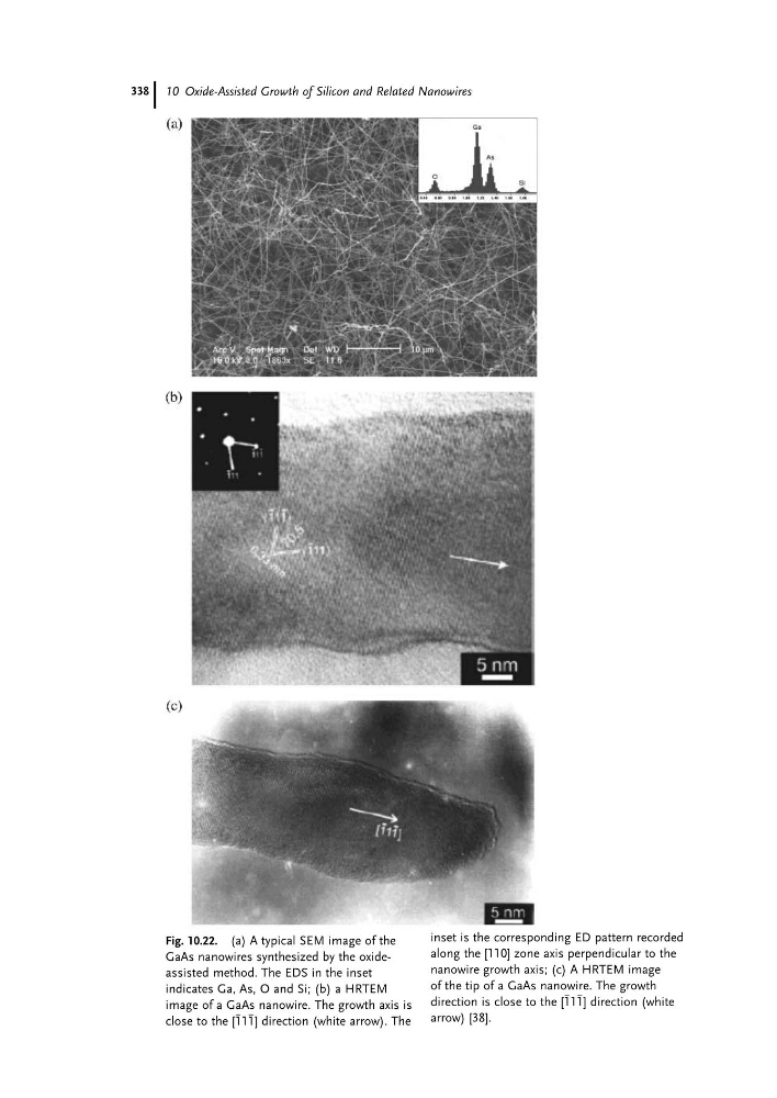
Fig. 10.22. (a) A typical SEM image of the
GaAs nanowires synthesized by the oxideassisted method. The EDS in the inset
indicates Ga, As, O and Si; (b) a HRTEM
image of a GaAs nanowire. The growth axis is
close to the [111] direction (white arrow). The
inset is the corresponding ED pattern recorded
along the [110] zone axis perpendicular to the
nanowire growth axis; (c) A HRTEM image
of the tip of a GaAs nanowire. The growth
direction is close to the [111] direction (white
arrow) [38].
10 Oxide-Assisted Growth of Silicon and Related Nanowires
338
GaAs nanowires synthesized by the oxideassisted method. The EDS in the inset
indicates Ga, As, O and Si; (b) a HRTEM
image of a GaAs nanowire. The growth axis is
close to the [111] direction (white arrow). The
inset is the corresponding ED pattern recorded
along the [110] zone axis perpendicular to the
nanowire growth axis; (c) A HRTEM image
of the tip of a GaAs nanowire. The growth
direction is close to the [111] direction (white
arrow) [38].
10 Oxide-Assisted Growth of Silicon and Related Nanowires
338