

vation (Figure 10.22(a)) shows that the product consists of wire-like structures with
length up to 10 mm and diameters of the order of 50 nm. The EDX spectrum
shown in the inset of this figure demonstrates that the nanowires consist only of
gallium, arsenic and oxygen. The silicon signal originates from the silicon substrate. HRTEM, selected-area electron diffraction (SAED) and electron energy-loss
spectrometry (EELS) of individual nanowires (Figure 10.22(b)) revealed a zincblende GaAs core enclosed in a gallium oxide (GaO x ) sheath. The [111] growth direction of the present nanowires is the same as that of GaAs nanowires grown by a
metal-catalyzed VLS process [72]. The diameter of the crystalline GaAs cores range
from 10 to 120 nm with the thickness of the outer sheath ranging from 2 to 10 nm.
The average diameter of the core was about 60 nm, and the average thickness of
the outer sheath was 5 nm. As expected from an OAG process, the crystalline GaAs
tip was coated with a thin amorphous layer of GaO x , similar to the SiO x tip of
SiNWs, and different from the GaAs nanowires synthesized by the metal catalyzed
VLS growth, in which the tips were terminated at metal-alloy nanoparticles [72].
We can thus suggest that the oxide-assisted nucleation and growth of GaAs
nanowires advances through the following reactions: (1) laser-induced decomposition of GaAs into Ga and As, (2) reaction of 4Ga þ Ga 2 O 3 ¼ 3Ga 2 O in the
high-temperature zone, (3) transport of volatile Ga 2 O and As to the lowtemperature-deposition zone, (4) reaction of 3Ga 2 O þ 4As ¼ 4GaAs þ Ga 2 O 3 in
the low-temperature-deposition zone leading to the nucleation and growth of the
GaAs nanowires.
The above model similarly applies to the successful synthesis of GaN and GaP
and other binary compounds. Figures 10.23 and 10.24 show the typical HRTEM
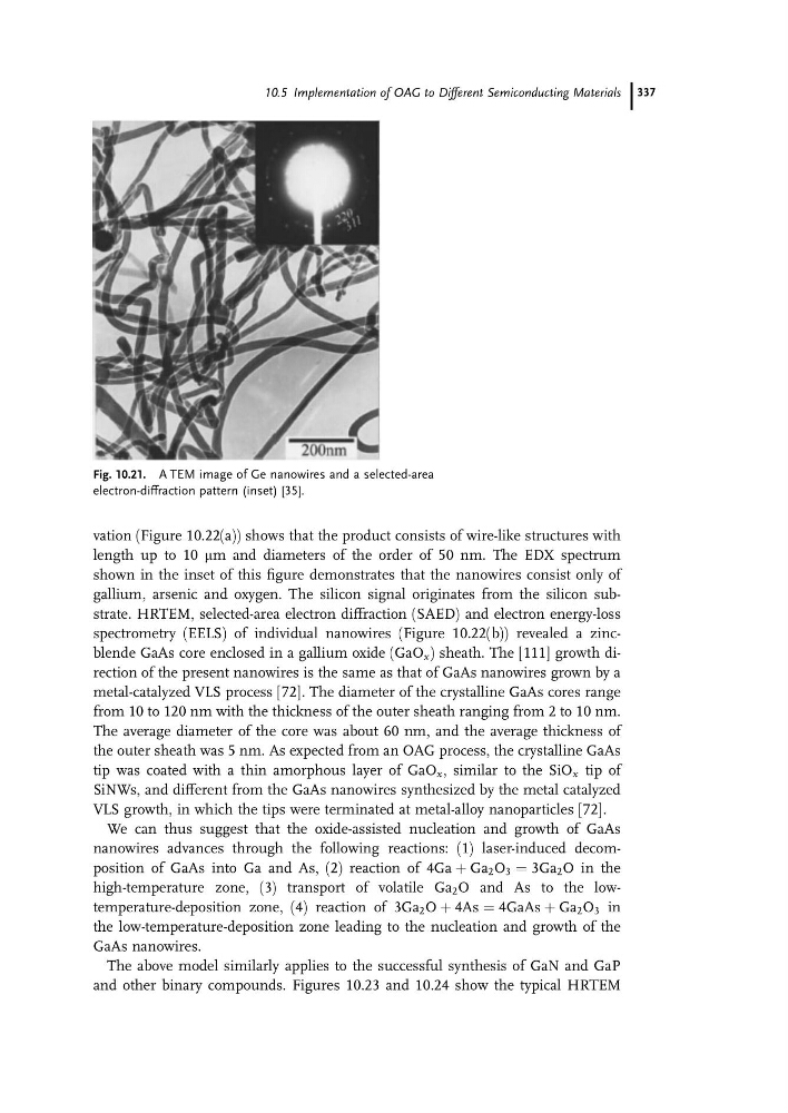
Fig. 10.21. A TEM image of Ge nanowires and a selected-area
electron-diffraction pattern (inset) [35].
10.5 Implementation of OAG to Different Semiconducting Materials 337
length up to 10 mm and diameters of the order of 50 nm. The EDX spectrum
shown in the inset of this figure demonstrates that the nanowires consist only of
gallium, arsenic and oxygen. The silicon signal originates from the silicon substrate. HRTEM, selected-area electron diffraction (SAED) and electron energy-loss
spectrometry (EELS) of individual nanowires (Figure 10.22(b)) revealed a zincblende GaAs core enclosed in a gallium oxide (GaO x ) sheath. The [111] growth direction of the present nanowires is the same as that of GaAs nanowires grown by a
metal-catalyzed VLS process [72]. The diameter of the crystalline GaAs cores range
from 10 to 120 nm with the thickness of the outer sheath ranging from 2 to 10 nm.
The average diameter of the core was about 60 nm, and the average thickness of
the outer sheath was 5 nm. As expected from an OAG process, the crystalline GaAs
tip was coated with a thin amorphous layer of GaO x , similar to the SiO x tip of
SiNWs, and different from the GaAs nanowires synthesized by the metal catalyzed
VLS growth, in which the tips were terminated at metal-alloy nanoparticles [72].
We can thus suggest that the oxide-assisted nucleation and growth of GaAs
nanowires advances through the following reactions: (1) laser-induced decomposition of GaAs into Ga and As, (2) reaction of 4Ga þ Ga 2 O 3 ¼ 3Ga 2 O in the
high-temperature zone, (3) transport of volatile Ga 2 O and As to the lowtemperature-deposition zone, (4) reaction of 3Ga 2 O þ 4As ¼ 4GaAs þ Ga 2 O 3 in
the low-temperature-deposition zone leading to the nucleation and growth of the
GaAs nanowires.
The above model similarly applies to the successful synthesis of GaN and GaP
and other binary compounds. Figures 10.23 and 10.24 show the typical HRTEM
Fig. 10.21. A TEM image of Ge nanowires and a selected-area
electron-diffraction pattern (inset) [35].
10.5 Implementation of OAG to Different Semiconducting Materials 337