

Similar to the production of Si nanowires, we used laser ablation of a mixed
GeO 2 /Ge target to synthesize Ge nanowires at 830
C. In comparison, Morales and
Lieber [21] used metal-containing targets for the same purpose. We show that Ge
nanowires are obtained by the OAG method in an analogous way to SiNWs. TEM
studies (Figure 10.21) show that the structure of the Ge nanowires is similar to that
of SiNWs, with a crystalline Ge core and a thick amorphous oxide shell. The diameters of the Ge nanowires in this particular experimental set-up had a larger
size distribution than that of SiNWs (ranging from 16 to 370 nm).
Gallium arsenide nanowires with a zinc-blende structure were fabricated by laser
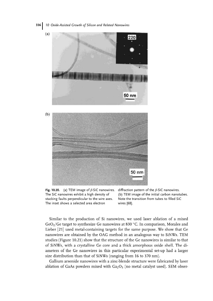
ablation of GaAs powders mixed with Ga 2 O 3 (no metal catalyst used). SEM obserFig. 10.20. (a) TEM image of b-SiC nanowires.
The SiC nanowires exhibit a high density of
stacking faults perpendicular to the wire axes.
The inset shows a selected area electron
diffraction pattern of the b-SiC nanowires.
(b) TEM image of the initial carbon nanotubes.
Note the transition from tubes to filled SiC
wires [68].
10 Oxide-Assisted Growth of Silicon and Related Nanowires
336
GeO 2 /Ge target to synthesize Ge nanowires at 830
C. In comparison, Morales and
Lieber [21] used metal-containing targets for the same purpose. We show that Ge
nanowires are obtained by the OAG method in an analogous way to SiNWs. TEM
studies (Figure 10.21) show that the structure of the Ge nanowires is similar to that
of SiNWs, with a crystalline Ge core and a thick amorphous oxide shell. The diameters of the Ge nanowires in this particular experimental set-up had a larger
size distribution than that of SiNWs (ranging from 16 to 370 nm).
Gallium arsenide nanowires with a zinc-blende structure were fabricated by laser
ablation of GaAs powders mixed with Ga 2 O 3 (no metal catalyst used). SEM obserFig. 10.20. (a) TEM image of b-SiC nanowires.
The SiC nanowires exhibit a high density of
stacking faults perpendicular to the wire axes.
The inset shows a selected area electron
diffraction pattern of the b-SiC nanowires.
(b) TEM image of the initial carbon nanotubes.
Note the transition from tubes to filled SiC
wires [68].
10 Oxide-Assisted Growth of Silicon and Related Nanowires
336