

synthesis of oriented SiC nanowires by reacting SiO with aligned carbon nanotubes prepared via the established method of pyrolysis of acetylene over film-like
iron/silica substrates [69, 70, 71]. Solid SiO powders (purity 99.9%) were placed in
a graphite crucible and covered with a molybdenum grid. The highly aligned carbon nanotubes were placed on the molybdenum grid. The crucible was covered
with a graphite lid, placed in the hot zone inside the alumina tube, and held in a
flowing argon atmosphere (50 sccm) at 1400
C for 2 h. After reaction, the aligned
carbon nanotube arrays were converted to oriented SiC nanowire arrays. These
highly oriented SiC nanowires were similar in appearance to the original aligned
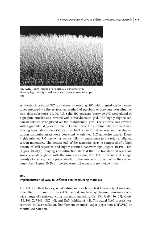
carbon nanotubes. The bottom end of the nanowire array is composed of a high
density of well-separated and highly oriented nanowire tips (Figure 10.19). TEM
(Figure 10.20(a)) imaging and diffraction showed that the transformed wires are
single crystalline b-SiC with the wire axes along the (111) direction and a high
density of stacking faults perpendicular to the wire axis. In contrast to the carbon
nanotubes (Figure 10.20(b)) the SiC were full wires and not hollow tubes.
10.5
Implementation of OAG to Different Semiconducting Materials
The OAG method has a general nature and can be applied to a variety of materials
other than Si. Based on the OAG method, we have synthesized nanowires of a
wide range of semiconducting materials including Ge [35], GaN [36, 37], GaAs
[38, 39], GaP [41], SiC [40], and ZnO (whiskers) [42]. The actual OAG process was
activated by laser ablation, hot-filament chemical vapor deposition (HFCVD) or
thermal evaporation.
Fig. 10.19. SEM images of oriented SiC nanowire array
showing high density of well-separated, oriented nanowire tips
[68].
10.5 Implementation of OAG to Different Semiconducting Materials 335
iron/silica substrates [69, 70, 71]. Solid SiO powders (purity 99.9%) were placed in
a graphite crucible and covered with a molybdenum grid. The highly aligned carbon nanotubes were placed on the molybdenum grid. The crucible was covered
with a graphite lid, placed in the hot zone inside the alumina tube, and held in a
flowing argon atmosphere (50 sccm) at 1400
C for 2 h. After reaction, the aligned
carbon nanotube arrays were converted to oriented SiC nanowire arrays. These
highly oriented SiC nanowires were similar in appearance to the original aligned
carbon nanotubes. The bottom end of the nanowire array is composed of a high
density of well-separated and highly oriented nanowire tips (Figure 10.19). TEM
(Figure 10.20(a)) imaging and diffraction showed that the transformed wires are
single crystalline b-SiC with the wire axes along the (111) direction and a high
density of stacking faults perpendicular to the wire axis. In contrast to the carbon
nanotubes (Figure 10.20(b)) the SiC were full wires and not hollow tubes.
10.5
Implementation of OAG to Different Semiconducting Materials
The OAG method has a general nature and can be applied to a variety of materials
other than Si. Based on the OAG method, we have synthesized nanowires of a
wide range of semiconducting materials including Ge [35], GaN [36, 37], GaAs
[38, 39], GaP [41], SiC [40], and ZnO (whiskers) [42]. The actual OAG process was
activated by laser ablation, hot-filament chemical vapor deposition (HFCVD) or
thermal evaporation.
Fig. 10.19. SEM images of oriented SiC nanowire array
showing high density of well-separated, oriented nanowire tips
[68].
10.5 Implementation of OAG to Different Semiconducting Materials 335