

10.4.2
Metal Silicide (MS)/SiNWs from Metal Vapor Vacuum Arc Implantation [67]
A conventional method to produce contacts in the semiconductor industry is ion
implantation. The possible advantages of ion implantation for SiNWs are in the
control in adding precise (and small) amounts of metal atoms to SiNWs, which
might be difficult for bulkier techniques. Here we describe ion implantation of
Ni and Co into 20 nm diameter SiNWs produced by thermal decomposition of SiO.
The SiNWs were mounted on copper folding grids and directly implanted by
metal vapor vacuum arc (MEVVA) implantation with a 5 keV Ni
þ or Co
þ dose of
1 Â 10
17 cm
À2 at room temperature. The implanted samples were later annealed
in argon.
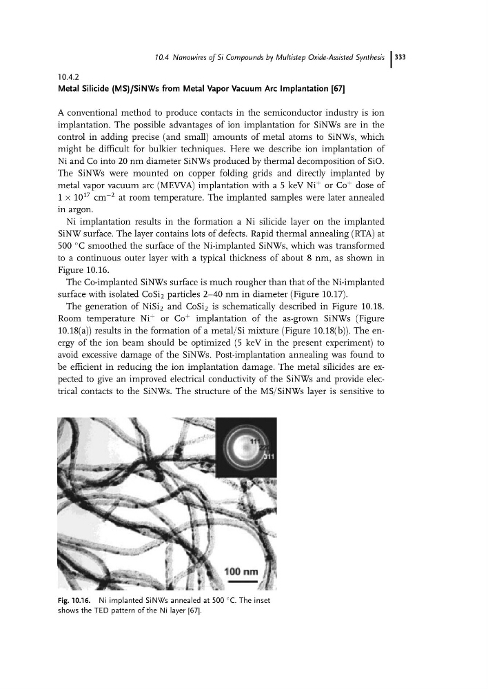
Ni implantation results in the formation a Ni silicide layer on the implanted
SiNW surface. The layer contains lots of defects. Rapid thermal annealing (RTA) at
500
C smoothed the surface of the Ni-implanted SiNWs, which was transformed
to a continuous outer layer with a typical thickness of about 8 nm, as shown in
Figure 10.16.
The Co-implanted SiNWs surface is much rougher than that of the Ni-implanted
surface with isolated CoSi 2 particles 2–40 nm in diameter (Figure 10.17).
The generation of NiSi 2 and CoSi 2 is schematically described in Figure 10.18.
Room temperature Ni
þ or Co
þ implantation of the as-grown SiNWs (Figure
10.18(a)) results in the formation of a metal/Si mixture (Figure 10.18(b)). The energy of the ion beam should be optimized (5 keV in the present experiment) to
avoid excessive damage of the SiNWs. Post-implantation annealing was found to
be efficient in reducing the ion implantation damage. The metal silicides are expected to give an improved electrical conductivity of the SiNWs and provide electrical contacts to the SiNWs. The structure of the MS/SiNWs layer is sensitive to
Fig. 10.16. Ni implanted SiNWs annealed at 500
C. The inset
shows the TED pattern of the Ni layer [67].
10.4 Nanowires of Si Compounds by Multistep Oxide-Assisted Synthesis 333
Metal Silicide (MS)/SiNWs from Metal Vapor Vacuum Arc Implantation [67]
A conventional method to produce contacts in the semiconductor industry is ion
implantation. The possible advantages of ion implantation for SiNWs are in the
control in adding precise (and small) amounts of metal atoms to SiNWs, which
might be difficult for bulkier techniques. Here we describe ion implantation of
Ni and Co into 20 nm diameter SiNWs produced by thermal decomposition of SiO.
The SiNWs were mounted on copper folding grids and directly implanted by
metal vapor vacuum arc (MEVVA) implantation with a 5 keV Ni
þ or Co
þ dose of
1 Â 10
17 cm
À2 at room temperature. The implanted samples were later annealed
in argon.
Ni implantation results in the formation a Ni silicide layer on the implanted
SiNW surface. The layer contains lots of defects. Rapid thermal annealing (RTA) at
500
C smoothed the surface of the Ni-implanted SiNWs, which was transformed
to a continuous outer layer with a typical thickness of about 8 nm, as shown in
Figure 10.16.
The Co-implanted SiNWs surface is much rougher than that of the Ni-implanted
surface with isolated CoSi 2 particles 2–40 nm in diameter (Figure 10.17).
The generation of NiSi 2 and CoSi 2 is schematically described in Figure 10.18.
Room temperature Ni
þ or Co
þ implantation of the as-grown SiNWs (Figure
10.18(a)) results in the formation of a metal/Si mixture (Figure 10.18(b)). The energy of the ion beam should be optimized (5 keV in the present experiment) to
avoid excessive damage of the SiNWs. Post-implantation annealing was found to
be efficient in reducing the ion implantation damage. The metal silicides are expected to give an improved electrical conductivity of the SiNWs and provide electrical contacts to the SiNWs. The structure of the MS/SiNWs layer is sensitive to
Fig. 10.16. Ni implanted SiNWs annealed at 500
C. The inset
shows the TED pattern of the Ni layer [67].
10.4 Nanowires of Si Compounds by Multistep Oxide-Assisted Synthesis 333