

growth kinetics along different crystallographic directions (i.e. two fast growing
directions).
10.4
Nanowires of Si Compounds by Multistep Oxide-Assisted Synthesis
10.4.1
Nanocables [65]
Coaxial three-layer cables offer a potentially simple way of producing nanojunctions. The idea of applying the nanocable configuration was indeed recently reported by Iijima et al. [66]. Such nanocables can be produced by a multistep process. We give as an example a coaxial three-layer nanocable synthesized by
combining high-temperature laser ablation of SiC as the first step, and thermal
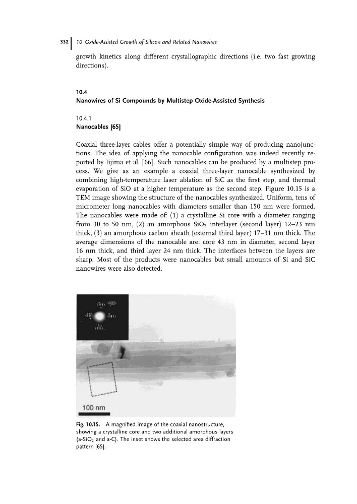
evaporation of SiO at a higher temperature as the second step. Figure 10.15 is a
TEM image showing the structure of the nanocables synthesized. Uniform, tens of
micrometer long nanocables with diameters smaller than 150 nm were formed.
The nanocables were made of: (1) a crystalline Si core with a diameter ranging
from 30 to 50 nm, (2) an amorphous SiO 2 interlayer (second layer) 12–23 nm
thick, (3) an amorphous carbon sheath (external third layer) 17–31 nm thick. The
average dimensions of the nanocable are: core 43 nm in diameter, second layer
16 nm thick, and third layer 24 nm thick. The interfaces between the layers are
sharp. Most of the products were nanocables but small amounts of Si and SiC
nanowires were also detected.
Fig. 10.15. A magnified image of the coaxial nanostructure,
showing a crystalline core and two additional amorphous layers
(a-SiO 2 and a-C). The inset shows the selected area diffraction
pattern [65].
10 Oxide-Assisted Growth of Silicon and Related Nanowires
332
directions).
10.4
Nanowires of Si Compounds by Multistep Oxide-Assisted Synthesis
10.4.1
Nanocables [65]
Coaxial three-layer cables offer a potentially simple way of producing nanojunctions. The idea of applying the nanocable configuration was indeed recently reported by Iijima et al. [66]. Such nanocables can be produced by a multistep process. We give as an example a coaxial three-layer nanocable synthesized by
combining high-temperature laser ablation of SiC as the first step, and thermal
evaporation of SiO at a higher temperature as the second step. Figure 10.15 is a
TEM image showing the structure of the nanocables synthesized. Uniform, tens of
micrometer long nanocables with diameters smaller than 150 nm were formed.
The nanocables were made of: (1) a crystalline Si core with a diameter ranging
from 30 to 50 nm, (2) an amorphous SiO 2 interlayer (second layer) 12–23 nm
thick, (3) an amorphous carbon sheath (external third layer) 17–31 nm thick. The
average dimensions of the nanocable are: core 43 nm in diameter, second layer
16 nm thick, and third layer 24 nm thick. The interfaces between the layers are
sharp. Most of the products were nanocables but small amounts of Si and SiC
nanowires were also detected.
Fig. 10.15. A magnified image of the coaxial nanostructure,
showing a crystalline core and two additional amorphous layers
(a-SiO 2 and a-C). The inset shows the selected area diffraction
pattern [65].
10 Oxide-Assisted Growth of Silicon and Related Nanowires
332