

direction common for the metal catalyst VLS growth. Most surprisingly, no evidence for metal particles was found either on the SiNWs tips or in the wires
themselves, regardless of the metal used in the target (Fe, Ni or Co), in sharp contrast to those SiNWs grown in the high-temperature region. The SiNW tips were
generally round and covered by a relatively thick Si oxide layer (2–3 nm) and no
other component other than Si or O was detected by electron energy dispersive
spectroscopy (EDS). The Si crystal core near the tip contained a high density of
stacking faults and micro-twins [27], generally along the nanowire axis in the
h112i direction.
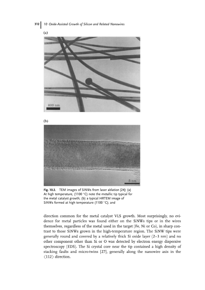
Fig. 10.2. TEM images of SiNWs from laser ablation [24]: (a)
At high temperature, (1100
C) note the metallic tip typical for
the metal catalyst growth; (b) a typical HRTEM image of
SiNWs formed at high temperature (1100
C); and
10 Oxide-Assisted Growth of Silicon and Related Nanowires
312
themselves, regardless of the metal used in the target (Fe, Ni or Co), in sharp contrast to those SiNWs grown in the high-temperature region. The SiNW tips were
generally round and covered by a relatively thick Si oxide layer (2–3 nm) and no
other component other than Si or O was detected by electron energy dispersive
spectroscopy (EDS). The Si crystal core near the tip contained a high density of
stacking faults and micro-twins [27], generally along the nanowire axis in the
h112i direction.
Fig. 10.2. TEM images of SiNWs from laser ablation [24]: (a)
At high temperature, (1100
C) note the metallic tip typical for
the metal catalyst growth; (b) a typical HRTEM image of
SiNWs formed at high temperature (1100
C); and
10 Oxide-Assisted Growth of Silicon and Related Nanowires
312