

10.2
Oxide-Assisted Nanowire Growth
10.2.1
Discovery of Oxide-Assisted Growth [23–25]
Si nanowires were first produced using the classical metal catalyst VLS approach
[21, 22, 46]. Laser ablation of a metal-containing Si target produces metal/metal
silicide nanoparticles that act as the critical catalyst needed for the nucleation of
SiNWs. The wires grow further by dissolution of silicon in the metallic nano-cap
and concurrent Si segregation from the cap. In a typical experiment, an excimer
laser is used to ablate the target placed in an evacuated quartz tube filled with an
inert gas, e.g. argon [22].
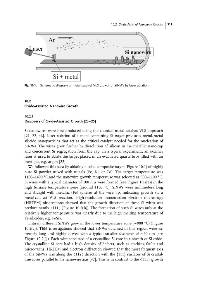
We followed this idea by ablating a solid composite target (Figure 10.1) of highly
pure Si powder mixed with metals (Fe, Ni, or Co). The target temperature was
1100–1400
C and the nanowire growth temperature was selected as 900–1100
C.
Si wires with a typical diameter of 100 nm were formed (see Figure 10.2(a)) in the
high furnace temperature zone (around 1100
C). SiNWs were millimeters long
and straight with metallic (Fe) spheres at the wire tip, indicating growth via a
metal-catalyst VLS reaction. High-resolution transmission electron microscopy
(HRTEM) observations showed that the growth direction of these Si wires was
predominantly h111i (Figure 10.2(b)). The formation of such Si wires only at the
relatively higher temperature was clearly due to the high melting temperature of
Fe-silicides, e.g. FeSi 2 .
Entirely different SiNWs grew in the lower temperature zone (@900
C) (Figure
10.2(c)). TEM investigations showed that SiNWs obtained in this region were extremely long and highly curved with a typical smaller diameter of @20 nm (see
Figure 10.2(). Each wire consisted of a crystalline Si core in a sheath of Si oxide.
The crystalline Si core had a high density of defects, such as stacking faults and
micro-twins. HRTEM and electron diffraction showed that the most frequent axis
of the SiNWs was along the h112i direction with the {111} surfaces of Si crystalline cores parallel to the nanowire axis [47]. This is in contrast to the h111i growth
Fig. 10.1. Schematic diagram of metal catalyst VLS growth of SiNWs by laser ablation.
10.2 Oxide-Assisted Nanowire Growth 311
Oxide-Assisted Nanowire Growth
10.2.1
Discovery of Oxide-Assisted Growth [23–25]
Si nanowires were first produced using the classical metal catalyst VLS approach
[21, 22, 46]. Laser ablation of a metal-containing Si target produces metal/metal
silicide nanoparticles that act as the critical catalyst needed for the nucleation of
SiNWs. The wires grow further by dissolution of silicon in the metallic nano-cap
and concurrent Si segregation from the cap. In a typical experiment, an excimer
laser is used to ablate the target placed in an evacuated quartz tube filled with an
inert gas, e.g. argon [22].
We followed this idea by ablating a solid composite target (Figure 10.1) of highly
pure Si powder mixed with metals (Fe, Ni, or Co). The target temperature was
1100–1400
C and the nanowire growth temperature was selected as 900–1100
C.
Si wires with a typical diameter of 100 nm were formed (see Figure 10.2(a)) in the
high furnace temperature zone (around 1100
C). SiNWs were millimeters long
and straight with metallic (Fe) spheres at the wire tip, indicating growth via a
metal-catalyst VLS reaction. High-resolution transmission electron microscopy
(HRTEM) observations showed that the growth direction of these Si wires was
predominantly h111i (Figure 10.2(b)). The formation of such Si wires only at the
relatively higher temperature was clearly due to the high melting temperature of
Fe-silicides, e.g. FeSi 2 .
Entirely different SiNWs grew in the lower temperature zone (@900
C) (Figure
10.2(c)). TEM investigations showed that SiNWs obtained in this region were extremely long and highly curved with a typical smaller diameter of @20 nm (see
Figure 10.2(). Each wire consisted of a crystalline Si core in a sheath of Si oxide.
The crystalline Si core had a high density of defects, such as stacking faults and
micro-twins. HRTEM and electron diffraction showed that the most frequent axis
of the SiNWs was along the h112i direction with the {111} surfaces of Si crystalline cores parallel to the nanowire axis [47]. This is in contrast to the h111i growth
Fig. 10.1. Schematic diagram of metal catalyst VLS growth of SiNWs by laser ablation.
10.2 Oxide-Assisted Nanowire Growth 311