

7.1 Basic Receiver Operation
275
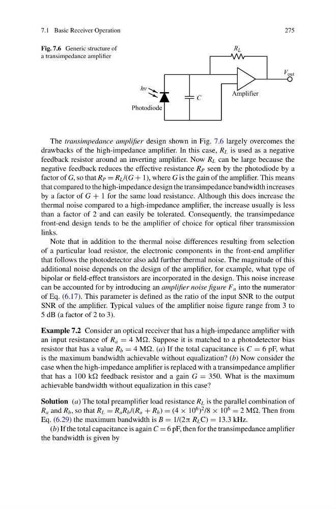
Fig. 7.6 Generic structure of
a transimpedance amplifier
The transimpedance amplifier design shown in Fig. 7.6 largely overcomes the
drawbacks of the high-impedance amplifier. In this case, R L is used as a negative
feedback resistor around an inverting amplifier. Now R L can be large because the
negative feedback reduces the effective resistance R P seen by the photodiode by a
factor of G, so that R P = R L /(G + 1), where G is the gain of the amplifier. This means
that compared to the high-impedance design the transimpedance bandwidth increases
by a factor of G + 1 for the same load resistance. Although this does increase the
thermal noise compared to a high-impedance amplifier, the increase usually is less
than a factor of 2 and can easily be tolerated. Consequently, the transimpedance
front-end design tends to be the amplifier of choice for optical fiber transmission
links.
Note that in addition to the thermal noise differences resulting from selection
of a particular load resistor, the electronic components in the front-end amplifier
that follows the photodetector also add further thermal noise. The magnitude of this
additional noise depends on the design of the amplifier, for example, what type of
bipolar or field-effect transistors are incorporated in the design. This noise increase
can be accounted for by introducing an amplifier noise figure F n into the numerator
of Eq. (6.17). This parameter is defined as the ratio of the input SNR to the output
SNR of the amplifier. Typical values of the amplifier noise figure range from 3 to
5 dB (a factor of 2 to 3).
Example 7.2 Consider an optical receiver that has a high-impedance amplifier with
an input resistance of R a = 4 M. Suppose it is matched to a photodetector bias
resistor that has a value R b = 4 M. (a) If the total capacitance is C = 6 pF, what
is the maximum bandwidth achievable without equalization? (b) Now consider the
case when the high-impedance amplifier is replaced with a transimpedance amplifier
that has a 100 k feedback resistor and a gain G = 350. What is the maximum
achievable bandwidth without equalization in this case?
Solution (a) The total preamplifier load resistance R L is the parallel combination of
R a and R b , so that R L = R a R b /(R a + R b ) = (4 × 10
6 )
2 /8 × 10
6
= 2 M. Then from
Eq. (6.29) the maximum bandwidth is B = 1/(2π R L C) = 13.3 kHz.
(b) If the total capacitance is again C = 6 pF, then for the transimpedance amplifier
the bandwidth is given by
275
Fig. 7.6 Generic structure of
a transimpedance amplifier
The transimpedance amplifier design shown in Fig. 7.6 largely overcomes the
drawbacks of the high-impedance amplifier. In this case, R L is used as a negative
feedback resistor around an inverting amplifier. Now R L can be large because the
negative feedback reduces the effective resistance R P seen by the photodiode by a
factor of G, so that R P = R L /(G + 1), where G is the gain of the amplifier. This means
that compared to the high-impedance design the transimpedance bandwidth increases
by a factor of G + 1 for the same load resistance. Although this does increase the
thermal noise compared to a high-impedance amplifier, the increase usually is less
than a factor of 2 and can easily be tolerated. Consequently, the transimpedance
front-end design tends to be the amplifier of choice for optical fiber transmission
links.
Note that in addition to the thermal noise differences resulting from selection
of a particular load resistor, the electronic components in the front-end amplifier
that follows the photodetector also add further thermal noise. The magnitude of this
additional noise depends on the design of the amplifier, for example, what type of
bipolar or field-effect transistors are incorporated in the design. This noise increase
can be accounted for by introducing an amplifier noise figure F n into the numerator
of Eq. (6.17). This parameter is defined as the ratio of the input SNR to the output
SNR of the amplifier. Typical values of the amplifier noise figure range from 3 to
5 dB (a factor of 2 to 3).
Example 7.2 Consider an optical receiver that has a high-impedance amplifier with
an input resistance of R a = 4 M. Suppose it is matched to a photodetector bias
resistor that has a value R b = 4 M. (a) If the total capacitance is C = 6 pF, what
is the maximum bandwidth achievable without equalization? (b) Now consider the
case when the high-impedance amplifier is replaced with a transimpedance amplifier
that has a 100 k feedback resistor and a gain G = 350. What is the maximum
achievable bandwidth without equalization in this case?
Solution (a) The total preamplifier load resistance R L is the parallel combination of
R a and R b , so that R L = R a R b /(R a + R b ) = (4 × 10
6 )
2 /8 × 10
6
= 2 M. Then from
Eq. (6.29) the maximum bandwidth is B = 1/(2π R L C) = 13.3 kHz.
(b) If the total capacitance is again C = 6 pF, then for the transimpedance amplifier
the bandwidth is given by