

6.3 Response Times of Photodiodes
261
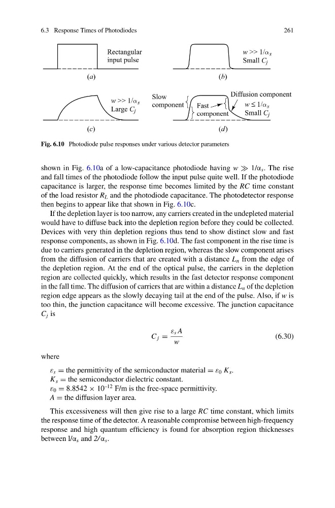
Fig. 6.10 Photodiode pulse responses under various detector parameters
shown in Fig. 6.10a of a low-capacitance photodiode having w 1/α s . The rise
and fall times of the photodiode follow the input pulse quite well. If the photodiode
capacitance is larger, the response time becomes limited by the RC time constant
of the load resistor R L and the photodiode capacitance. The photodetector response
then begins to appear like that shown in Fig. 6.10c.
If the depletion layer is too narrow, any carriers created in the undepleted material
would have to diffuse back into the depletion region before they could be collected.
Devices with very thin depletion regions thus tend to show distinct slow and fast
response components, as shown in Fig. 6.10d. The fast component in the rise time is
due to carriers generated in the depletion region, whereas the slow component arises
from the diffusion of carriers that are created with a distance L n from the edge of
the depletion region. At the end of the optical pulse, the carriers in the depletion
region are collected quickly, which results in the fast detector response component
in the fall time. The diffusion of carriers that are within a distance L n of the depletion
region edge appears as the slowly decaying tail at the end of the pulse. Also, if w is
too thin, the junction capacitance will become excessive. The junction capacitance
C j is
C j =
ε s A
w
(6.30)
where
ε s = the permittivity of the semiconductor material = ε 0 K s .
K s = the semiconductor dielectric constant.
ε 0 = 8.8542 × 10
–12 F/m is the free-space permittivity.
A = the diffusion layer area.
This excessiveness will then give rise to a large RC time constant, which limits
the response time of the detector. A reasonable compromise between high-frequency
response and high quantum efficiency is found for absorption region thicknesses
between l/α s and 2/ α s .
261
Fig. 6.10 Photodiode pulse responses under various detector parameters
shown in Fig. 6.10a of a low-capacitance photodiode having w 1/α s . The rise
and fall times of the photodiode follow the input pulse quite well. If the photodiode
capacitance is larger, the response time becomes limited by the RC time constant
of the load resistor R L and the photodiode capacitance. The photodetector response
then begins to appear like that shown in Fig. 6.10c.
If the depletion layer is too narrow, any carriers created in the undepleted material
would have to diffuse back into the depletion region before they could be collected.
Devices with very thin depletion regions thus tend to show distinct slow and fast
response components, as shown in Fig. 6.10d. The fast component in the rise time is
due to carriers generated in the depletion region, whereas the slow component arises
from the diffusion of carriers that are created with a distance L n from the edge of
the depletion region. At the end of the optical pulse, the carriers in the depletion
region are collected quickly, which results in the fast detector response component
in the fall time. The diffusion of carriers that are within a distance L n of the depletion
region edge appears as the slowly decaying tail at the end of the pulse. Also, if w is
too thin, the junction capacitance will become excessive. The junction capacitance
C j is
C j =
ε s A
w
(6.30)
where
ε s = the permittivity of the semiconductor material = ε 0 K s .
K s = the semiconductor dielectric constant.
ε 0 = 8.8542 × 10
–12 F/m is the free-space permittivity.
A = the diffusion layer area.
This excessiveness will then give rise to a large RC time constant, which limits
the response time of the detector. A reasonable compromise between high-frequency
response and high quantum efficiency is found for absorption region thicknesses
between l/α s and 2/ α s .