

260
6 Photodetection Devices
be generated in the depletion region or so close to it that the diffusion times are less
than or equal to the carrier drift times. The effect of long diffusion times can be
seen by considering the photodiode response time. This response time is described
by the rise time and fall time of the detector output when the detector is illuminated
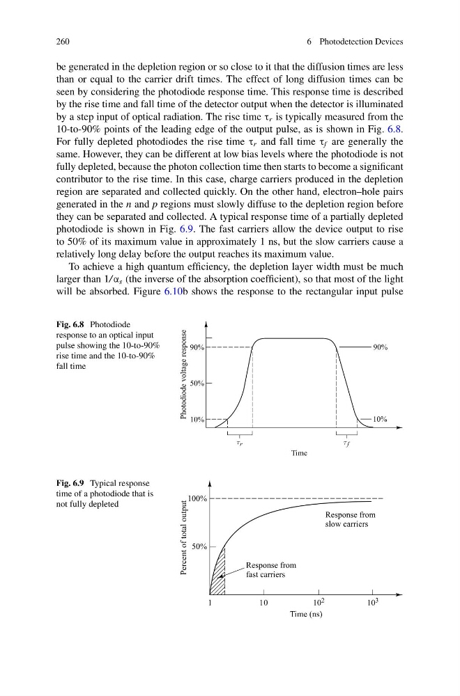
by a step input of optical radiation. The rise time τ r is typically measured from the
10-to-90% points of the leading edge of the output pulse, as is shown in Fig. 6.8.
For fully depleted photodiodes the rise time τ r and fall time τ f are generally the
same. However, they can be different at low bias levels where the photodiode is not
fully depleted, because the photon collection time then starts to become a significant
contributor to the rise time. In this case, charge carriers produced in the depletion
region are separated and collected quickly. On the other hand, electron–hole pairs
generated in the n and p regions must slowly diffuse to the depletion region before
they can be separated and collected. A typical response time of a partially depleted
photodiode is shown in Fig. 6.9. The fast carriers allow the device output to rise
to 50% of its maximum value in approximately 1 ns, but the slow carriers cause a
relatively long delay before the output reaches its maximum value.
To achieve a high quantum efficiency, the depletion layer width must be much
larger than 1/ α s (the inverse of the absorption coefficient), so that most of the light
will be absorbed. Figure 6.10b shows the response to the rectangular input pulse
Fig. 6.8 Photodiode
response to an optical input
pulse showing the 10-to-90%
rise time and the 10-to-90%
fall time
Fig. 6.9 Typical response
time of a photodiode that is
not fully depleted
6 Photodetection Devices
be generated in the depletion region or so close to it that the diffusion times are less
than or equal to the carrier drift times. The effect of long diffusion times can be
seen by considering the photodiode response time. This response time is described
by the rise time and fall time of the detector output when the detector is illuminated
by a step input of optical radiation. The rise time τ r is typically measured from the
10-to-90% points of the leading edge of the output pulse, as is shown in Fig. 6.8.
For fully depleted photodiodes the rise time τ r and fall time τ f are generally the
same. However, they can be different at low bias levels where the photodiode is not
fully depleted, because the photon collection time then starts to become a significant
contributor to the rise time. In this case, charge carriers produced in the depletion
region are separated and collected quickly. On the other hand, electron–hole pairs
generated in the n and p regions must slowly diffuse to the depletion region before
they can be separated and collected. A typical response time of a partially depleted
photodiode is shown in Fig. 6.9. The fast carriers allow the device output to rise
to 50% of its maximum value in approximately 1 ns, but the slow carriers cause a
relatively long delay before the output reaches its maximum value.
To achieve a high quantum efficiency, the depletion layer width must be much
larger than 1/ α s (the inverse of the absorption coefficient), so that most of the light
will be absorbed. Figure 6.10b shows the response to the rectangular input pulse
Fig. 6.8 Photodiode
response to an optical input
pulse showing the 10-to-90%
rise time and the 10-to-90%
fall time
Fig. 6.9 Typical response
time of a photodiode that is
not fully depleted