

6.3 Response Times of Photodiodes
259
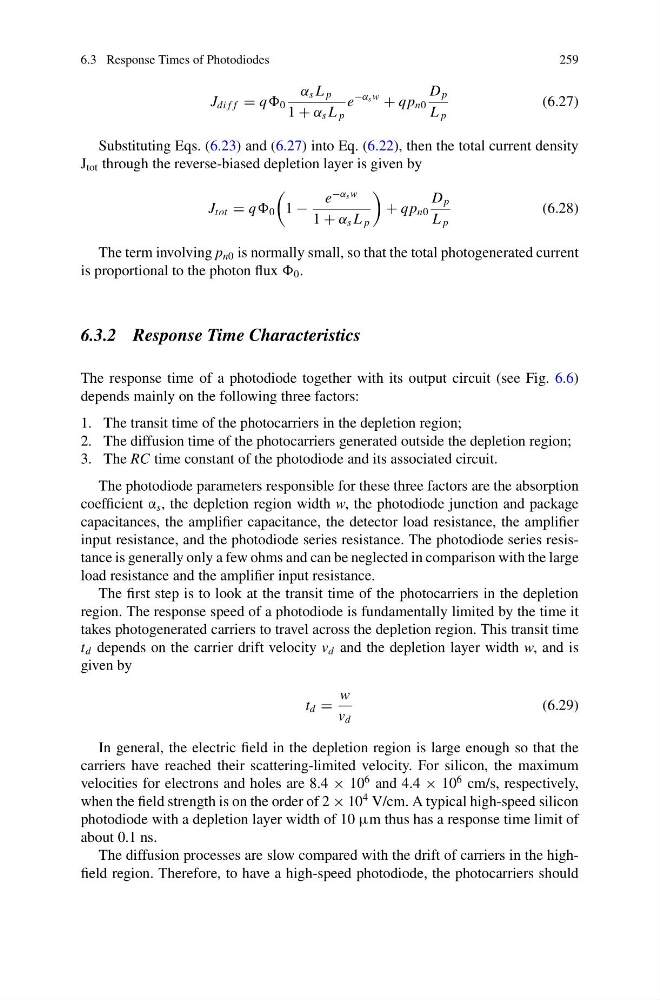
J di f f = q 0
α s L p
1 + α s L p
e
−α s w
+ qp n0
D p
L p
(6.27)
Substituting Eqs. (6.23) and (6.27) into Eq. (6.22), then the total current density
J tot through the reverse-biased depletion layer is given by
J tot = q 0
1 −
e
−α s w
1 + α s L p
+ qp n0
D p
L p
(6.28)
The term involving p n0 is normally small, so that the total photogenerated current
is proportional to the photon flux 0 .
6.3.2 Response Time Characteristics
The response time of a photodiode together with its output circuit (see Fig. 6.6)
depends mainly on the following three factors:
1. The transit time of the photocarriers in the depletion region;
2. The diffusion time of the photocarriers generated outside the depletion region;
3. The RC time constant of the photodiode and its associated circuit.
The photodiode parameters responsible for these three factors are the absorption
coefficient α s , the depletion region width w, the photodiode junction and package
capacitances, the amplifier capacitance, the detector load resistance, the amplifier
input resistance, and the photodiode series resistance. The photodiode series resistance is generally only a few ohms and can be neglected in comparison with the large
load resistance and the amplifier input resistance.
The first step is to look at the transit time of the photocarriers in the depletion
region. The response speed of a photodiode is fundamentally limited by the time it
takes photogenerated carriers to travel across the depletion region. This transit time
t d depends on the carrier drift velocity v d and the depletion layer width w, and is
given by
t d =
w
v d
(6.29)
In general, the electric field in the depletion region is large enough so that the
carriers have reached their scattering-limited velocity. For silicon, the maximum
velocities for electrons and holes are 8.4 × 10
6 and 4.4 × 10
6 cm/s, respectively,
when the field strength is on the order of 2 × 10
4 V/cm. A typical high-speed silicon
photodiode with a depletion layer width of 10 μm thus has a response time limit of
about 0.1 ns.
The diffusion processes are slow compared with the drift of carriers in the highfield region. Therefore, to have a high-speed photodiode, the photocarriers should
259
J di f f = q 0
α s L p
1 + α s L p
e
−α s w
+ qp n0
D p
L p
(6.27)
Substituting Eqs. (6.23) and (6.27) into Eq. (6.22), then the total current density
J tot through the reverse-biased depletion layer is given by
J tot = q 0
1 −
e
−α s w
1 + α s L p
+ qp n0
D p
L p
(6.28)
The term involving p n0 is normally small, so that the total photogenerated current
is proportional to the photon flux 0 .
6.3.2 Response Time Characteristics
The response time of a photodiode together with its output circuit (see Fig. 6.6)
depends mainly on the following three factors:
1. The transit time of the photocarriers in the depletion region;
2. The diffusion time of the photocarriers generated outside the depletion region;
3. The RC time constant of the photodiode and its associated circuit.
The photodiode parameters responsible for these three factors are the absorption
coefficient α s , the depletion region width w, the photodiode junction and package
capacitances, the amplifier capacitance, the detector load resistance, the amplifier
input resistance, and the photodiode series resistance. The photodiode series resistance is generally only a few ohms and can be neglected in comparison with the large
load resistance and the amplifier input resistance.
The first step is to look at the transit time of the photocarriers in the depletion
region. The response speed of a photodiode is fundamentally limited by the time it
takes photogenerated carriers to travel across the depletion region. This transit time
t d depends on the carrier drift velocity v d and the depletion layer width w, and is
given by
t d =
w
v d
(6.29)
In general, the electric field in the depletion region is large enough so that the
carriers have reached their scattering-limited velocity. For silicon, the maximum
velocities for electrons and holes are 8.4 × 10
6 and 4.4 × 10
6 cm/s, respectively,
when the field strength is on the order of 2 × 10
4 V/cm. A typical high-speed silicon
photodiode with a depletion layer width of 10 μm thus has a response time limit of
about 0.1 ns.
The diffusion processes are slow compared with the drift of carriers in the highfield region. Therefore, to have a high-speed photodiode, the photocarriers should