

246
6 Photodetection Devices
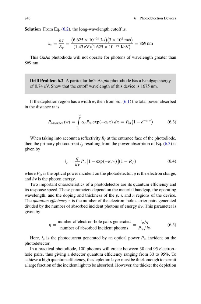
Solution From Eq. (6.2), the long-wavelength cutoff is.
λ c =
hc
E g
=
6.625 × 10
−34 J-s
3 × 10
8 m/s
(1.43 eV)
1.625 × 10 −19 J/eV
= 869 nm
This GaAs photodiode will not operate for photons of wavelength greater than
869 nm.
Drill Problem 6.2 A particular InGaAs pin photodiode has a bandgap energy
of 0.74 eV. Show that the cutoff wavelength of this device is 1675 nm.
If the depletion region has a width w, then from Eq. (6.1) the total power absorbed
in the distance w is
P absorbed (w) =
w
0
α s P in exp(−α s x) dx = P in
1 − e
−α s w
(6.3)
When taking into account a reflectivity R f at the entrance face of the photodiode,
then the primary photocurrent i p resulting from the power absorption of Eq. (6.3) is
given by
i p =
q
hν
P in
1 − exp(−α s w)
1 − R f
(6.4)
where P in is the optical power incident on the photodetector, q is the electron charge,
and hν is the photon energy.
Two important characteristics of a photodetector are its quantum efficiency and
its response speed. These parameters depend on the material bandgap, the operating
wavelength, and the doping and thickness of the p, i, and n regions of the device.
The quantum efficiency η is the number of the electron–hole carrier pairs generated
divided by the number of absorbed incident photons of energy hν. This parameter is
given by
η =
number of electron-hole pairs generated
number of absorbed incident photons
=
i p /q
P in / hν
(6.5)
Here, i p is the photocurrent generated by an optical power P in incident on the
photodetector.
In a practical photodiode, 100 photons will create between 30 and 95 electron–
hole pairs, thus giving a detector quantum efficiency ranging from 30 to 95%. To
achieve a high quantum efficiency, the depletion layer must be thick enough to permit
a large fraction of the incident light to be absorbed. However, the thicker the depletion
6 Photodetection Devices
Solution From Eq. (6.2), the long-wavelength cutoff is.
λ c =
hc
E g
=
6.625 × 10
−34 J-s
3 × 10
8 m/s
(1.43 eV)
1.625 × 10 −19 J/eV
= 869 nm
This GaAs photodiode will not operate for photons of wavelength greater than
869 nm.
Drill Problem 6.2 A particular InGaAs pin photodiode has a bandgap energy
of 0.74 eV. Show that the cutoff wavelength of this device is 1675 nm.
If the depletion region has a width w, then from Eq. (6.1) the total power absorbed
in the distance w is
P absorbed (w) =
w
0
α s P in exp(−α s x) dx = P in
1 − e
−α s w
(6.3)
When taking into account a reflectivity R f at the entrance face of the photodiode,
then the primary photocurrent i p resulting from the power absorption of Eq. (6.3) is
given by
i p =
q
hν
P in
1 − exp(−α s w)
1 − R f
(6.4)
where P in is the optical power incident on the photodetector, q is the electron charge,
and hν is the photon energy.
Two important characteristics of a photodetector are its quantum efficiency and
its response speed. These parameters depend on the material bandgap, the operating
wavelength, and the doping and thickness of the p, i, and n regions of the device.
The quantum efficiency η is the number of the electron–hole carrier pairs generated
divided by the number of absorbed incident photons of energy hν. This parameter is
given by
η =
number of electron-hole pairs generated
number of absorbed incident photons
=
i p /q
P in / hν
(6.5)
Here, i p is the photocurrent generated by an optical power P in incident on the
photodetector.
In a practical photodiode, 100 photons will create between 30 and 95 electron–
hole pairs, thus giving a detector quantum efficiency ranging from 30 to 95%. To
achieve a high quantum efficiency, the depletion layer must be thick enough to permit
a large fraction of the incident light to be absorbed. However, the thicker the depletion