

4.1 Basic Concepts of Semiconductor Physics
151
exp
1.42 × 1.6 × 10
−19
2
1.381 × 10 −23
300
= 2.62 × 10
12 m
−3
= 2.62 × 10
6 cm
−3
Drill Problem 4.1 The effective masses for Si are m e = 1.09 m and m h = 0.56 m
for electrons and holes, respectively, where m is the electron rest mass given
in Example 4.1. Using Eq. (4.1) show that the intrinsic carrier concentration is
n = p = n i = 1.00 × 10
10 cm
−3 . To get an accurate value of the ratio E g /2k B T
for the exponential factor in Eq. (4.1), use the values E g = 1.100 eV and 2k B T
= 0.02586 eV at T = 300 °K.
The conduction in Si can be greatly increased by adding traces of impurities
from the group V elements (e.g., P, As, Sb). This process is called doping, and the
doped semiconductor is called an extrinsic material. These doping elements have five
electrons in the outer shell. When they replace a Si atom, four electrons are used for
covalent bonding, and the fifth, loosely bound electron is available for conduction. As
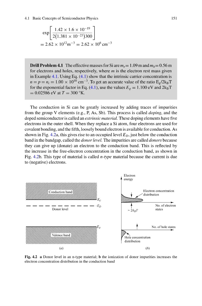
shown in Fig. 4.2a, this gives rise to an occupied level E D , just below the conduction
band in the bandgap, called the donor level. The impurities are called donors because
they can give up (donate) an electron to the conduction band. This is reflected by
the increase in the free-electron concentration in the conduction band, as shown in
Fig. 4.2b. This type of material is called n-type material because the current is due
to (negative) electrons.
Fig. 4.2 a Donor level in an n-type material; b the ionization of donor impurities increases the
electron concentration distribution in the conduction band
151
exp
1.42 × 1.6 × 10
−19
2
1.381 × 10 −23
300
= 2.62 × 10
12 m
−3
= 2.62 × 10
6 cm
−3
Drill Problem 4.1 The effective masses for Si are m e = 1.09 m and m h = 0.56 m
for electrons and holes, respectively, where m is the electron rest mass given
in Example 4.1. Using Eq. (4.1) show that the intrinsic carrier concentration is
n = p = n i = 1.00 × 10
10 cm
−3 . To get an accurate value of the ratio E g /2k B T
for the exponential factor in Eq. (4.1), use the values E g = 1.100 eV and 2k B T
= 0.02586 eV at T = 300 °K.
The conduction in Si can be greatly increased by adding traces of impurities
from the group V elements (e.g., P, As, Sb). This process is called doping, and the
doped semiconductor is called an extrinsic material. These doping elements have five
electrons in the outer shell. When they replace a Si atom, four electrons are used for
covalent bonding, and the fifth, loosely bound electron is available for conduction. As
shown in Fig. 4.2a, this gives rise to an occupied level E D , just below the conduction
band in the bandgap, called the donor level. The impurities are called donors because
they can give up (donate) an electron to the conduction band. This is reflected by
the increase in the free-electron concentration in the conduction band, as shown in
Fig. 4.2b. This type of material is called n-type material because the current is due
to (negative) electrons.
Fig. 4.2 a Donor level in an n-type material; b the ionization of donor impurities increases the
electron concentration distribution in the conduction band