

152
4 Light Sources for Fiber Links
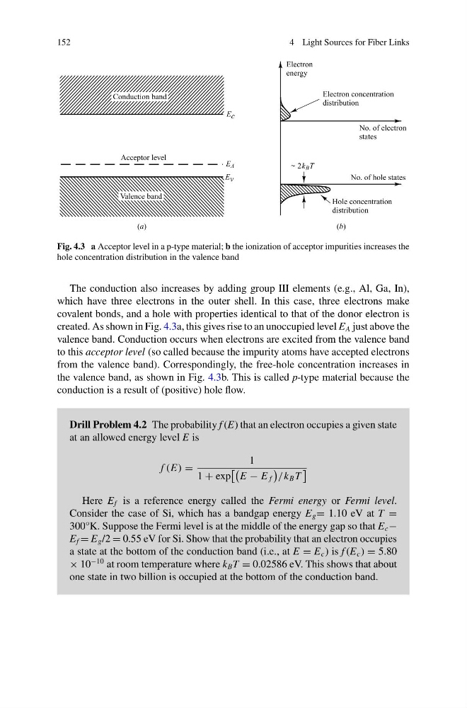
Fig. 4.3 a Acceptor level in a p-type material; b the ionization of acceptor impurities increases the
hole concentration distribution in the valence band
The conduction also increases by adding group III elements (e.g., Al, Ga, In),
which have three electrons in the outer shell. In this case, three electrons make
covalent bonds, and a hole with properties identical to that of the donor electron is
created. As shown in Fig. 4.3a, this gives rise to an unoccupied level E A just above the
valence band. Conduction occurs when electrons are excited from the valence band
to this acceptor level (so called because the impurity atoms have accepted electrons
from the valence band). Correspondingly, the free-hole concentration increases in
the valence band, as shown in Fig. 4.3b. This is called p-type material because the
conduction is a result of (positive) hole flow.
Drill Problem 4.2 The probability f (E) that an electron occupies a given state
at an allowed energy level E is
f (E) =
1
1 + exp
E − E f
/k B T
Here E f is a reference energy called the Fermi energy or Fermi level.
Consider the case of Si, which has a bandgap energy E g = 1.10 eV at T =
300°K. Suppose the Fermi level is at the middle of the energy gap so that E c −
E f = E g /2 = 0.55 eV for Si. Show that the probability that an electron occupies
a state at the bottom of the conduction band (i.e., at E = E c ) is f (E c ) = 5.80
× 10
−10 at room temperature where k B T = 0.02586 eV. This shows that about
one state in two billion is occupied at the bottom of the conduction band.
4 Light Sources for Fiber Links
Fig. 4.3 a Acceptor level in a p-type material; b the ionization of acceptor impurities increases the
hole concentration distribution in the valence band
The conduction also increases by adding group III elements (e.g., Al, Ga, In),
which have three electrons in the outer shell. In this case, three electrons make
covalent bonds, and a hole with properties identical to that of the donor electron is
created. As shown in Fig. 4.3a, this gives rise to an unoccupied level E A just above the
valence band. Conduction occurs when electrons are excited from the valence band
to this acceptor level (so called because the impurity atoms have accepted electrons
from the valence band). Correspondingly, the free-hole concentration increases in
the valence band, as shown in Fig. 4.3b. This is called p-type material because the
conduction is a result of (positive) hole flow.
Drill Problem 4.2 The probability f (E) that an electron occupies a given state
at an allowed energy level E is
f (E) =
1
1 + exp
E − E f
/k B T
Here E f is a reference energy called the Fermi energy or Fermi level.
Consider the case of Si, which has a bandgap energy E g = 1.10 eV at T =
300°K. Suppose the Fermi level is at the middle of the energy gap so that E c −
E f = E g /2 = 0.55 eV for Si. Show that the probability that an electron occupies
a state at the bottom of the conduction band (i.e., at E = E c ) is f (E c ) = 5.80
× 10
−10 at room temperature where k B T = 0.02586 eV. This shows that about
one state in two billion is occupied at the bottom of the conduction band.