

150
4 Light Sources for Fiber Links
hole. This action makes the hole move in the opposite direction to the electron flow,
as is shown in Fig. 4.1a.
When an electron propagates in a semiconductor, it interacts with the periodically
arranged constituent atoms of the material and thus experiences external forces. As a
result, to describe its acceleration a crys in a semiconductor crystal under an external
force F ext its mass needs to be described by a quantum mechanical quantity m e called
the effective mass. That is, when using the relationship F ext = m e a crys (force equals
mass times acceleration), the effects of all the forces exerted on the electron within
the material are incorporated into m e .
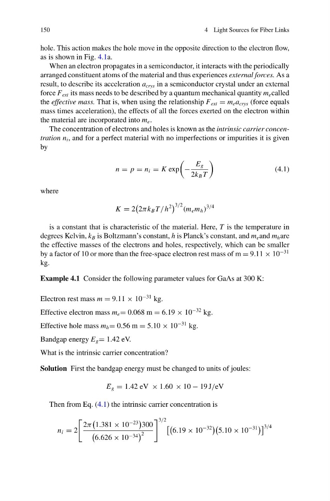
The concentration of electrons and holes is known as the intrinsic carrier concentration n i , and for a perfect material with no imperfections or impurities it is given
by
n = p = n i = K exp
−
E g
2k B T
(4.1)
where
K = 2
2π k B T / h
2
3/2 (m e m h )
3/4
is a constant that is characteristic of the material. Here, T is the temperature in
degrees Kelvin, k B is Boltzmann’s constant, h is Planck’s constant, and m e and m h are
the effective masses of the electrons and holes, respectively, which can be smaller
by a factor of 10 or more than the free-space electron rest mass of m = 9.11 × 10
−31
kg.
Example 4.1 Consider the following parameter values for GaAs at 300 K:
Electron rest mass m = 9.11 × 10
−31 kg.
Effective electron mass m e = 0.068 m = 6.19 × 10
−32 kg.
Effective hole mass m h = 0.56 m = 5.10 × 10
−31 kg.
Bandgap energy E g = 1.42 eV.
What is the intrinsic carrier concentration?
Solution First the bandgap energy must be changed to units of joules:
E g = 1.42 eV × 1.60 × 10 − 19 J/eV
Then from Eq. (4.1) the intrinsic carrier concentration is
n i = 2
2π
1.381 × 10
−23
300
6.626 × 10 −34
2
3/2
6.19 × 10
−32
5.10 × 10
−31
3/4
4 Light Sources for Fiber Links
hole. This action makes the hole move in the opposite direction to the electron flow,
as is shown in Fig. 4.1a.
When an electron propagates in a semiconductor, it interacts with the periodically
arranged constituent atoms of the material and thus experiences external forces. As a
result, to describe its acceleration a crys in a semiconductor crystal under an external
force F ext its mass needs to be described by a quantum mechanical quantity m e called
the effective mass. That is, when using the relationship F ext = m e a crys (force equals
mass times acceleration), the effects of all the forces exerted on the electron within
the material are incorporated into m e .
The concentration of electrons and holes is known as the intrinsic carrier concentration n i , and for a perfect material with no imperfections or impurities it is given
by
n = p = n i = K exp
−
E g
2k B T
(4.1)
where
K = 2
2π k B T / h
2
3/2 (m e m h )
3/4
is a constant that is characteristic of the material. Here, T is the temperature in
degrees Kelvin, k B is Boltzmann’s constant, h is Planck’s constant, and m e and m h are
the effective masses of the electrons and holes, respectively, which can be smaller
by a factor of 10 or more than the free-space electron rest mass of m = 9.11 × 10
−31
kg.
Example 4.1 Consider the following parameter values for GaAs at 300 K:
Electron rest mass m = 9.11 × 10
−31 kg.
Effective electron mass m e = 0.068 m = 6.19 × 10
−32 kg.
Effective hole mass m h = 0.56 m = 5.10 × 10
−31 kg.
Bandgap energy E g = 1.42 eV.
What is the intrinsic carrier concentration?
Solution First the bandgap energy must be changed to units of joules:
E g = 1.42 eV × 1.60 × 10 − 19 J/eV
Then from Eq. (4.1) the intrinsic carrier concentration is
n i = 2
2π
1.381 × 10
−23
300
6.626 × 10 −34
2
3/2
6.19 × 10
−32
5.10 × 10
−31
3/4