

562
S. Yagi
demands for OLEDs are expected according to development of “Internet of Things
(IoT)”.
Emitting materials are one of the key constituents to determine the device performance of OLEDs, such as device efficiencies and chromaticity coordinates of electroluminescence (EL). The first report of EL from an organic compound was done
in 1960s (Helfrich and Schneider 1965, 1966). Therein, although EL was obtained
from a single crystalline anthracene, extremely high voltage was applied to it due to
poor charge carrier injection. The prototype device structure of the current OLEDs
was reported in 1987 by Tang and VanSlyke, which achieved high luminance of
more than 1000 cd m
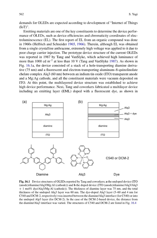
–2 at less than 10 V (Tang and VanSlyke 1987). As shown in
Fig. 16.1a, the device consisted of a stack of a hole-transporting diamine derivative (75 nm) and a fluorescent and electron-transporting aluminum–8-quinolinolate
chelate complex Alq3 (60 nm) between an indium tin oxide (ITO) transparent anode
and a Mg:Ag cathode, and all the constituent materials were vacuum deposited on
ITO. At this point, the multilayered device structure was established to achieve
high device performance. Next, Tang and coworkers fabricated a multilayer device
including an emitting layer (EML) doped with a fluorescent dye, as shown in
Fig. 16.1 Device structures of OLEDs reported by Tang and coworkers; a the undoped device (ITO
(anode)/diamine/Alq3/Mg:Al (cathode)) and b the doped device (ITO (anode)/diamine/Alq3/Alq3
+ 1 mol% dye/Alq3/Mg:Al (cathode)). The thickness of diamine layer was 75 nm, and the total
thickness of the undoped Alq3 layer was 60 nm. The dye-doped Alq3 layer (5–60 and 4 nm for
C540 and DCM-2, respectively) was inserted between the diamine/Alq3 interface (for C540) or into
the undoped Alp3 layer (for DCM-2). In the case of the DCM-2-based device, the distance from
the diamine/Alq3 interface was varied. The structures of C540 and DCM-2 are listed in Fig. 16.4
S. Yagi
demands for OLEDs are expected according to development of “Internet of Things
(IoT)”.
Emitting materials are one of the key constituents to determine the device performance of OLEDs, such as device efficiencies and chromaticity coordinates of electroluminescence (EL). The first report of EL from an organic compound was done
in 1960s (Helfrich and Schneider 1965, 1966). Therein, although EL was obtained
from a single crystalline anthracene, extremely high voltage was applied to it due to
poor charge carrier injection. The prototype device structure of the current OLEDs
was reported in 1987 by Tang and VanSlyke, which achieved high luminance of
more than 1000 cd m
–2 at less than 10 V (Tang and VanSlyke 1987). As shown in
Fig. 16.1a, the device consisted of a stack of a hole-transporting diamine derivative (75 nm) and a fluorescent and electron-transporting aluminum–8-quinolinolate
chelate complex Alq3 (60 nm) between an indium tin oxide (ITO) transparent anode
and a Mg:Ag cathode, and all the constituent materials were vacuum deposited on
ITO. At this point, the multilayered device structure was established to achieve
high device performance. Next, Tang and coworkers fabricated a multilayer device
including an emitting layer (EML) doped with a fluorescent dye, as shown in
Fig. 16.1 Device structures of OLEDs reported by Tang and coworkers; a the undoped device (ITO
(anode)/diamine/Alq3/Mg:Al (cathode)) and b the doped device (ITO (anode)/diamine/Alq3/Alq3
+ 1 mol% dye/Alq3/Mg:Al (cathode)). The thickness of diamine layer was 75 nm, and the total
thickness of the undoped Alq3 layer was 60 nm. The dye-doped Alq3 layer (5–60 and 4 nm for
C540 and DCM-2, respectively) was inserted between the diamine/Alq3 interface (for C540) or into
the undoped Alp3 layer (for DCM-2). In the case of the DCM-2-based device, the distance from
the diamine/Alq3 interface was varied. The structures of C540 and DCM-2 are listed in Fig. 16.4