

many times, in conjunction with deposition of multiple materials, in order
to build complex structures such as integrated circuits. The technique
excels at creating regular, patterned surfaces, and the process produces
surfaces fairly quickly, but the fabrication of the mask can be difficult.
As mentioned above, the resolution of the pattern is determined by the
wavelength of light. Usually UV light is used to create patterns down to
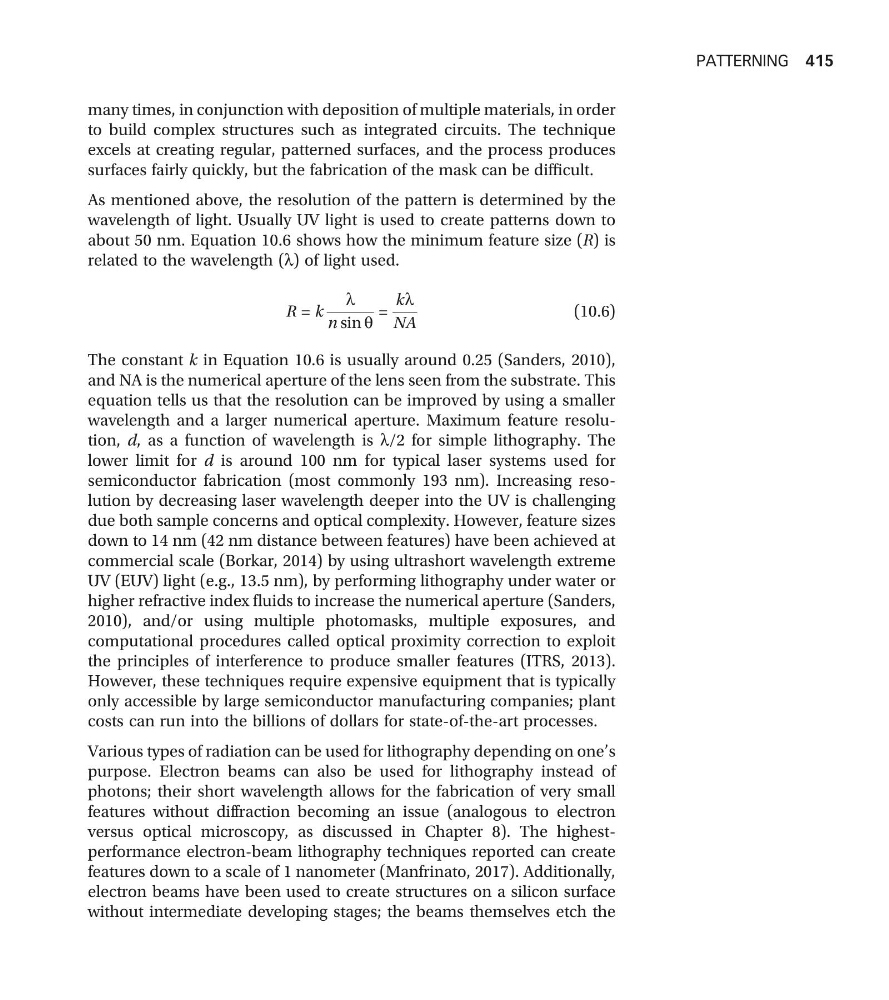
about 50 nm. Equation 10.6 shows how the minimum feature size (R) is
related to the wavelength (l) of light used.
R = k
l
n sin q
=
kl
NA
(10.6)
The constant k in Equation 10.6 is usually around 0.25 (Sanders, 2010),
and NA is the numerical aperture of the lens seen from the substrate. This
equation tells us that the resolution can be improved by using a smaller
wavelength and a larger numerical aperture. Maximum feature resolution, d, as a function of wavelength is l/2 for simple lithography. The
lower limit for d is around 100 nm for typical laser systems used for
semiconductor fabrication (most commonly 193 nm). Increasing resolution by decreasing laser wavelength deeper into the UV is challenging
due both sample concerns and optical complexity. However, feature sizes
down to 14 nm (42 nm distance between features) have been achieved at
commercial scale (Borkar, 2014) by using ultrashort wavelength extreme
UV (EUV) light (e.g., 13.5 nm), by performing lithography under water or
higher refractive index fluids to increase the numerical aperture (Sanders,
2010), and/or using multiple photomasks, multiple exposures, and
computational procedures called optical proximity correction to exploit
the principles of interference to produce smaller features (ITRS, 2013).
However, these techniques require expensive equipment that is typically
only accessible by large semiconductor manufacturing companies; plant
costs can run into the billions of dollars for state-of-the-art processes.
Various types of radiation can be used for lithography depending on one’s
purpose. Electron beams can also be used for lithography instead of
photons; their short wavelength allows for the fabrication of very small
features without diffraction becoming an issue (analogous to electron
versus optical microscopy, as discussed in Chapter 8). The highestperformance electron-beam lithography techniques reported can create
features down to a scale of 1 nanometer (Manfrinato, 2017). Additionally,
electron beams have been used to create structures on a silicon surface
without intermediate developing stages; the beams themselves etch the
PATTERNING 415
to build complex structures such as integrated circuits. The technique
excels at creating regular, patterned surfaces, and the process produces
surfaces fairly quickly, but the fabrication of the mask can be difficult.
As mentioned above, the resolution of the pattern is determined by the
wavelength of light. Usually UV light is used to create patterns down to
about 50 nm. Equation 10.6 shows how the minimum feature size (R) is
related to the wavelength (l) of light used.
R = k
l
n sin q
=
kl
NA
(10.6)
The constant k in Equation 10.6 is usually around 0.25 (Sanders, 2010),
and NA is the numerical aperture of the lens seen from the substrate. This
equation tells us that the resolution can be improved by using a smaller
wavelength and a larger numerical aperture. Maximum feature resolution, d, as a function of wavelength is l/2 for simple lithography. The
lower limit for d is around 100 nm for typical laser systems used for
semiconductor fabrication (most commonly 193 nm). Increasing resolution by decreasing laser wavelength deeper into the UV is challenging
due both sample concerns and optical complexity. However, feature sizes
down to 14 nm (42 nm distance between features) have been achieved at
commercial scale (Borkar, 2014) by using ultrashort wavelength extreme
UV (EUV) light (e.g., 13.5 nm), by performing lithography under water or
higher refractive index fluids to increase the numerical aperture (Sanders,
2010), and/or using multiple photomasks, multiple exposures, and
computational procedures called optical proximity correction to exploit
the principles of interference to produce smaller features (ITRS, 2013).
However, these techniques require expensive equipment that is typically
only accessible by large semiconductor manufacturing companies; plant
costs can run into the billions of dollars for state-of-the-art processes.
Various types of radiation can be used for lithography depending on one’s
purpose. Electron beams can also be used for lithography instead of
photons; their short wavelength allows for the fabrication of very small
features without diffraction becoming an issue (analogous to electron
versus optical microscopy, as discussed in Chapter 8). The highestperformance electron-beam lithography techniques reported can create
features down to a scale of 1 nanometer (Manfrinato, 2017). Additionally,
electron beams have been used to create structures on a silicon surface
without intermediate developing stages; the beams themselves etch the
PATTERNING 415