

10.6.1 Optical and electron beam lithography
One important method is optical lithography (or photolithography),
which is a method capable of producing nanoscale patterns using very
short wavelength lasers. The wavelength of light determines the resolution of the nanopattern. For example, using a single exposure and single
lithography mask in vacuum, UV lithography at 193 nm can reach a
resolution of about 100 nm, while x-ray lithography can reach a resolution
of ~15 nm by using light of wavelength ~1 nm. However, resolution can be
enhanced via a variety of techniques, and lithography on features below
the diffraction limit is an active field of research.
Photolithography can be performed with either a photomask placed
directly on a substrate (contact lithography) or using light focused through
a photomask onto a substrate using a specialized projector called a
stepper. Higher precision and smaller features can be obtained with a
stepper than with contact lithography; however, steppers are very
expensive, such that contract lithography is more common for laboratoryscale fabrication. For either type of lithography, the region to be patterned
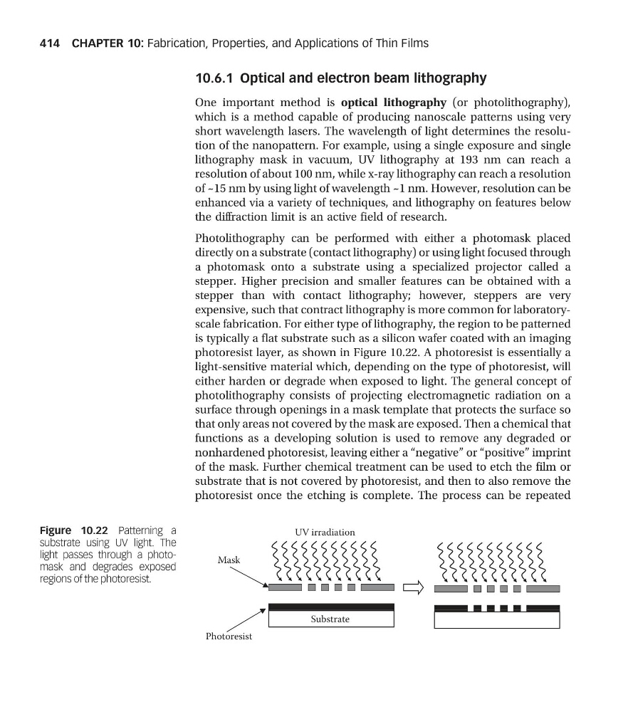
is typically a flat substrate such as a silicon wafer coated with an imaging
photoresist layer, as shown in Figure 10.22. A photoresist is essentially a
light-sensitive material which, depending on the type of photoresist, will
either harden or degrade when exposed to light. The general concept of
photolithography consists of projecting electromagnetic radiation on a
surface through openings in a mask template that protects the surface so
that only areas not covered by the mask are exposed. Then a chemical that
functions as a developing solution is used to remove any degraded or
nonhardened photoresist, leaving either a “negative” or “positive” imprint
of the mask. Further chemical treatment can be used to etch the film or
substrate that is not covered by photoresist, and then to also remove the
photoresist once the etching is complete. The process can be repeated
UV irradiation
Mask
Substrate
Photoresist
Figure 10.22 Patterning a
substrate using UV light. The
light passes through a photomask and degrades exposed
regions of the photoresist.
CHAPTER 10: Fabrication, Properties, and Applications of Thin Films
414
One important method is optical lithography (or photolithography),
which is a method capable of producing nanoscale patterns using very
short wavelength lasers. The wavelength of light determines the resolution of the nanopattern. For example, using a single exposure and single
lithography mask in vacuum, UV lithography at 193 nm can reach a
resolution of about 100 nm, while x-ray lithography can reach a resolution
of ~15 nm by using light of wavelength ~1 nm. However, resolution can be
enhanced via a variety of techniques, and lithography on features below
the diffraction limit is an active field of research.
Photolithography can be performed with either a photomask placed
directly on a substrate (contact lithography) or using light focused through
a photomask onto a substrate using a specialized projector called a
stepper. Higher precision and smaller features can be obtained with a
stepper than with contact lithography; however, steppers are very
expensive, such that contract lithography is more common for laboratoryscale fabrication. For either type of lithography, the region to be patterned
is typically a flat substrate such as a silicon wafer coated with an imaging
photoresist layer, as shown in Figure 10.22. A photoresist is essentially a
light-sensitive material which, depending on the type of photoresist, will
either harden or degrade when exposed to light. The general concept of
photolithography consists of projecting electromagnetic radiation on a
surface through openings in a mask template that protects the surface so
that only areas not covered by the mask are exposed. Then a chemical that
functions as a developing solution is used to remove any degraded or
nonhardened photoresist, leaving either a “negative” or “positive” imprint
of the mask. Further chemical treatment can be used to etch the film or
substrate that is not covered by photoresist, and then to also remove the
photoresist once the etching is complete. The process can be repeated
UV irradiation
Mask
Substrate
Photoresist
Figure 10.22 Patterning a
substrate using UV light. The
light passes through a photomask and degrades exposed
regions of the photoresist.
CHAPTER 10: Fabrication, Properties, and Applications of Thin Films
414