

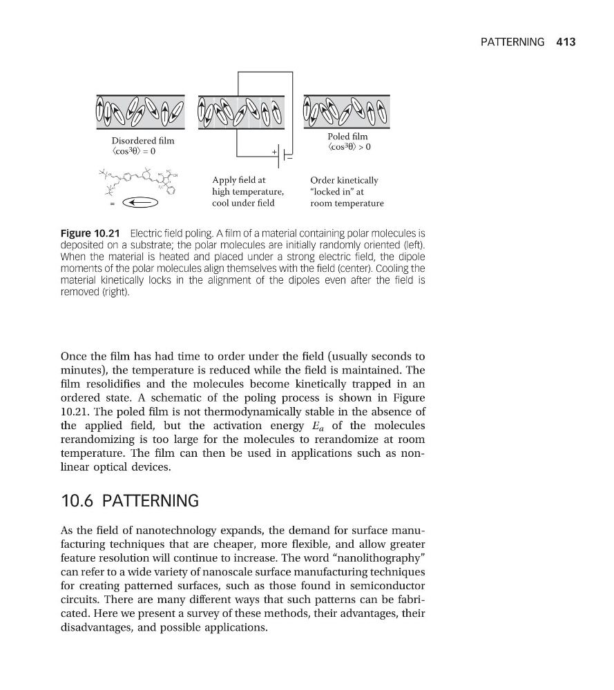
Once the film has had time to order under the field (usually seconds to
minutes), the temperature is reduced while the field is maintained. The
film resolidifies and the molecules become kinetically trapped in an
ordered state. A schematic of the poling process is shown in Figure
10.21. The poled film is not thermodynamically stable in the absence of
the applied field, but the activation energy E a of the molecules
rerandomizing is too large for the molecules to rerandomize at room
temperature. The film can then be used in applications such as nonlinear optical devices.
10.6 PATTERNING
As the field of nanotechnology expands, the demand for surface manufacturing techniques that are cheaper, more flexible, and allow greater
feature resolution will continue to increase. The word “nanolithography”
can refer to a wide variety of nanoscale surface manufacturing techniques
for creating patterned surfaces, such as those found in semiconductor
circuits. There are many different ways that such patterns can be fabricated. Here we present a survey of these methods, their advantages, their
disadvantages, and possible applications.
=
Apply field at
high temperature,
cool under field
Disordered film
cos 3 θ = 0
Poled film
cos 3 θ > 0
Order kinetically
“locked in” at
room temperature
+ –
Si
Si
O
O
N
NC
NC
CN
O
F 3C
Figure 10.21 Electric field poling. A film of a material containing polar molecules is
deposited on a substrate; the polar molecules are initially randomly oriented (left).
When the material is heated and placed under a strong electric field, the dipole
moments of the polar molecules align themselves with the field (center). Cooling the
material kinetically locks in the alignment of the dipoles even after the field is
removed (right).
PATTERNING 413
minutes), the temperature is reduced while the field is maintained. The
film resolidifies and the molecules become kinetically trapped in an
ordered state. A schematic of the poling process is shown in Figure
10.21. The poled film is not thermodynamically stable in the absence of
the applied field, but the activation energy E a of the molecules
rerandomizing is too large for the molecules to rerandomize at room
temperature. The film can then be used in applications such as nonlinear optical devices.
10.6 PATTERNING
As the field of nanotechnology expands, the demand for surface manufacturing techniques that are cheaper, more flexible, and allow greater
feature resolution will continue to increase. The word “nanolithography”
can refer to a wide variety of nanoscale surface manufacturing techniques
for creating patterned surfaces, such as those found in semiconductor
circuits. There are many different ways that such patterns can be fabricated. Here we present a survey of these methods, their advantages, their
disadvantages, and possible applications.
=
Apply field at
high temperature,
cool under field
Disordered film
cos 3 θ = 0
Poled film
cos 3 θ > 0
Order kinetically
“locked in” at
room temperature
+ –
Si
Si
O
O
N
NC
NC
CN
O
F 3C
Figure 10.21 Electric field poling. A film of a material containing polar molecules is
deposited on a substrate; the polar molecules are initially randomly oriented (left).
When the material is heated and placed under a strong electric field, the dipole
moments of the polar molecules align themselves with the field (center). Cooling the
material kinetically locks in the alignment of the dipoles even after the field is
removed (right).
PATTERNING 413