

micrometer (10
−6 m). Regardless, the typical nanowire has a width-tolength ratio of 1:1000 or more, allowing the structure to be viewed as onedimensional (1D). Combined with the comparatively small size of
nanowires, the 1D structure is responsible for the unique properties that
grossly distinguish nanowires from the average (three-dimensional) wire.
The potential applications for nanowires are immense. As technology
continues to advance, the trend in industry is to generate smaller but
more powerful electronic devices than previously sold on the market. As a
result, computer components such as resistors, capacitors, and circuits
continue to shrink. To link these components, increasingly small wires are
desired. There is also great interest in nanowires from the battery
industry, since the high surface area of nanowire arrays relative to bulk
metals could lead to more efficient anodes and cathodes. Industries also
see the potential for nanowires in such applications as chemical composites, field emitters, and biomolecular nanosensor leads. Moreover,
nanowires’ conductance can be controlled by synthesizing the wire from
any one of a variety of substrates, allowing for nanowires to have more
specialized roles. As a result, nanowires are categorized as (in order of
increasing conductance ability) insulators (SiO 2 , TiO 2 ), semiconductors (Si, GaN, InP), or metallics (Au, Cu, Pt, Ni, etc.). With such major
SC
14:16
000000 MD 9.0 mm 15.0 kV ×15k
2 μm
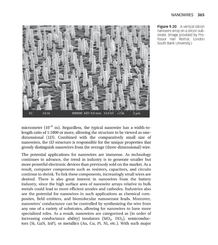
Figure 9.20 A vertical silicon
nanowire array on a silicon substrate. (Image provided by Professor Hari Reehal, London
South Bank University.)
NANOWIRES 365
−6 m). Regardless, the typical nanowire has a width-tolength ratio of 1:1000 or more, allowing the structure to be viewed as onedimensional (1D). Combined with the comparatively small size of
nanowires, the 1D structure is responsible for the unique properties that
grossly distinguish nanowires from the average (three-dimensional) wire.
The potential applications for nanowires are immense. As technology
continues to advance, the trend in industry is to generate smaller but
more powerful electronic devices than previously sold on the market. As a
result, computer components such as resistors, capacitors, and circuits
continue to shrink. To link these components, increasingly small wires are
desired. There is also great interest in nanowires from the battery
industry, since the high surface area of nanowire arrays relative to bulk
metals could lead to more efficient anodes and cathodes. Industries also
see the potential for nanowires in such applications as chemical composites, field emitters, and biomolecular nanosensor leads. Moreover,
nanowires’ conductance can be controlled by synthesizing the wire from
any one of a variety of substrates, allowing for nanowires to have more
specialized roles. As a result, nanowires are categorized as (in order of
increasing conductance ability) insulators (SiO 2 , TiO 2 ), semiconductors (Si, GaN, InP), or metallics (Au, Cu, Pt, Ni, etc.). With such major
SC
14:16
000000 MD 9.0 mm 15.0 kV ×15k
2 μm
Figure 9.20 A vertical silicon
nanowire array on a silicon substrate. (Image provided by Professor Hari Reehal, London
South Bank University.)
NANOWIRES 365