

are transmitted through a thin sample to produce an image. For our
current discussion, we focus on TEM as a tool to image nanomaterials.
8.7.3.1 Principles of TEM
The resolution of an image produced by an optical microscope is limited by
the wavelength of the radiation being used. If we use the Abbe equation
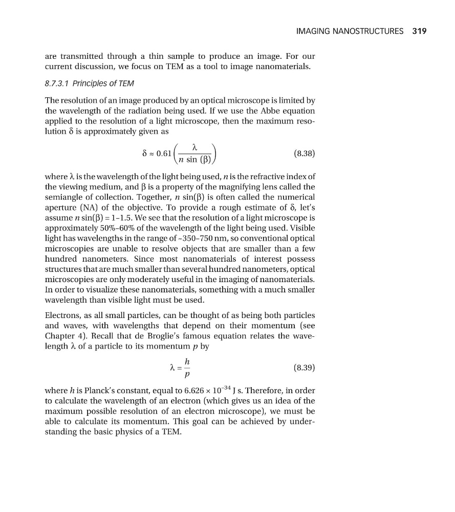
applied to the resolution of a light microscope, then the maximum resolution d is approximately given as
d ≈ 0:61
l
n sin (b)
(8.38)
where l is the wavelength of the light being used, n is the refractive index of
the viewing medium, and b is a property of the magnifying lens called the
semiangle of collection. Together, n sin(b) is often called the numerical
aperture (NA) of the objective. To provide a rough estimate of d, let’s
assume n sin(b) = 1–1.5. We see that the resolution of a light microscope is
approximately 50%–60% of the wavelength of the light being used. Visible
light has wavelengths in the range of ~350–750 nm, so conventional optical
microscopies are unable to resolve objects that are smaller than a few
hundred nanometers. Since most nanomaterials of interest possess
structures that are much smaller than several hundred nanometers, optical
microscopies are only moderately useful in the imaging of nanomaterials.
In order to visualize these nanomaterials, something with a much smaller
wavelength than visible light must be used.
Electrons, as all small particles, can be thought of as being both particles
and waves, with wavelengths that depend on their momentum (see
Chapter 4). Recall that de Broglie’s famous equation relates the wavelength l of a particle to its momentum p by
l =
h
p
(8.39)
where h is Planck’s constant, equal to 6.626 × 10
–34 J s. Therefore, in order
to calculate the wavelength of an electron (which gives us an idea of the
maximum possible resolution of an electron microscope), we must be
able to calculate its momentum. This goal can be achieved by understanding the basic physics of a TEM.
IMAGING NANOSTRUCTURES 319
current discussion, we focus on TEM as a tool to image nanomaterials.
8.7.3.1 Principles of TEM
The resolution of an image produced by an optical microscope is limited by
the wavelength of the radiation being used. If we use the Abbe equation
applied to the resolution of a light microscope, then the maximum resolution d is approximately given as
d ≈ 0:61
l
n sin (b)
(8.38)
where l is the wavelength of the light being used, n is the refractive index of
the viewing medium, and b is a property of the magnifying lens called the
semiangle of collection. Together, n sin(b) is often called the numerical
aperture (NA) of the objective. To provide a rough estimate of d, let’s
assume n sin(b) = 1–1.5. We see that the resolution of a light microscope is
approximately 50%–60% of the wavelength of the light being used. Visible
light has wavelengths in the range of ~350–750 nm, so conventional optical
microscopies are unable to resolve objects that are smaller than a few
hundred nanometers. Since most nanomaterials of interest possess
structures that are much smaller than several hundred nanometers, optical
microscopies are only moderately useful in the imaging of nanomaterials.
In order to visualize these nanomaterials, something with a much smaller
wavelength than visible light must be used.
Electrons, as all small particles, can be thought of as being both particles
and waves, with wavelengths that depend on their momentum (see
Chapter 4). Recall that de Broglie’s famous equation relates the wavelength l of a particle to its momentum p by
l =
h
p
(8.39)
where h is Planck’s constant, equal to 6.626 × 10
–34 J s. Therefore, in order
to calculate the wavelength of an electron (which gives us an idea of the
maximum possible resolution of an electron microscope), we must be
able to calculate its momentum. This goal can be achieved by understanding the basic physics of a TEM.
IMAGING NANOSTRUCTURES 319