

8.7.2.2 Atomic force microscopy
Atomic force microscopy, or AFM, operates on principles similar to those
of STM. As with STM, AFM functions by scanning a sharp tip across a
surface to generate an image. However, rather than monitoring the tunneling current between the tip and the surface, AFM monitors the height
of the tip as it physically interacts with the surface at a constant force.
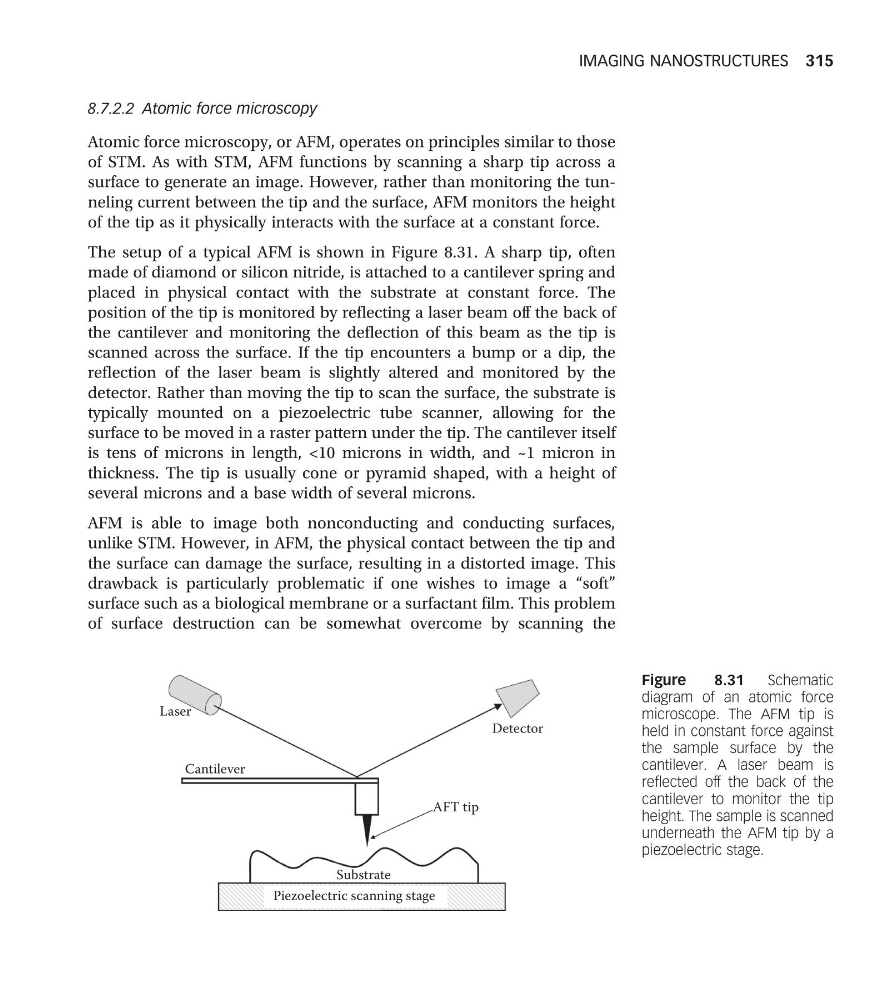
The setup of a typical AFM is shown in Figure 8.31. A sharp tip, often
made of diamond or silicon nitride, is attached to a cantilever spring and
placed in physical contact with the substrate at constant force. The
position of the tip is monitored by reflecting a laser beam off the back of
the cantilever and monitoring the deflection of this beam as the tip is
scanned across the surface. If the tip encounters a bump or a dip, the
reflection of the laser beam is slightly altered and monitored by the
detector. Rather than moving the tip to scan the surface, the substrate is
typically mounted on a piezoelectric tube scanner, allowing for the
surface to be moved in a raster pattern under the tip. The cantilever itself
is tens of microns in length, <10 microns in width, and ~1 micron in
thickness. The tip is usually cone or pyramid shaped, with a height of
several microns and a base width of several microns.
AFM is able to image both nonconducting and conducting surfaces,
unlike STM. However, in AFM, the physical contact between the tip and
the surface can damage the surface, resulting in a distorted image. This
drawback is particularly problematic if one wishes to image a “soft”
surface such as a biological membrane or a surfactant film. This problem
of surface destruction can be somewhat overcome by scanning the
Piezoelectric scanning stage
Substrate
AFT tip
Cantilever
Laser
Detector
Figure
8.31
Schematic
diagram of an atomic force
microscope. The AFM tip is
held in constant force against
the sample surface by the
cantilever. A laser beam is
reflected off the back of the
cantilever to monitor the tip
height. The sample is scanned
underneath the AFM tip by a
piezoelectric stage.
IMAGING NANOSTRUCTURES 315
Atomic force microscopy, or AFM, operates on principles similar to those
of STM. As with STM, AFM functions by scanning a sharp tip across a
surface to generate an image. However, rather than monitoring the tunneling current between the tip and the surface, AFM monitors the height
of the tip as it physically interacts with the surface at a constant force.
The setup of a typical AFM is shown in Figure 8.31. A sharp tip, often
made of diamond or silicon nitride, is attached to a cantilever spring and
placed in physical contact with the substrate at constant force. The
position of the tip is monitored by reflecting a laser beam off the back of
the cantilever and monitoring the deflection of this beam as the tip is
scanned across the surface. If the tip encounters a bump or a dip, the
reflection of the laser beam is slightly altered and monitored by the
detector. Rather than moving the tip to scan the surface, the substrate is
typically mounted on a piezoelectric tube scanner, allowing for the
surface to be moved in a raster pattern under the tip. The cantilever itself
is tens of microns in length, <10 microns in width, and ~1 micron in
thickness. The tip is usually cone or pyramid shaped, with a height of
several microns and a base width of several microns.
AFM is able to image both nonconducting and conducting surfaces,
unlike STM. However, in AFM, the physical contact between the tip and
the surface can damage the surface, resulting in a distorted image. This
drawback is particularly problematic if one wishes to image a “soft”
surface such as a biological membrane or a surfactant film. This problem
of surface destruction can be somewhat overcome by scanning the
Piezoelectric scanning stage
Substrate
AFT tip
Cantilever
Laser
Detector
Figure
8.31
Schematic
diagram of an atomic force
microscope. The AFM tip is
held in constant force against
the sample surface by the
cantilever. A laser beam is
reflected off the back of the
cantilever to monitor the tip
height. The sample is scanned
underneath the AFM tip by a
piezoelectric stage.
IMAGING NANOSTRUCTURES 315