

While such resolutions constitute a major achievement, STM suffers from
its inability to image surfaces that do not conduct electricity. Nonconducting surfaces are unable to be imaged unless they are modified or
coated with a conducting substance, which may damage the sample.
Atomic force microscopy, discussed below, does not suffer from this
disadvantage, although STM provides superior resolution.
For a typical STM, the lateral range of the scanner is generally from tens
of angstroms to approximately 100 µm. The allowable height is from
the sub-angstrom to ∼10 µm range. The tip is generally constructed
by manually cutting a platinum wire or by electrochemical etching of
tungsten metal.
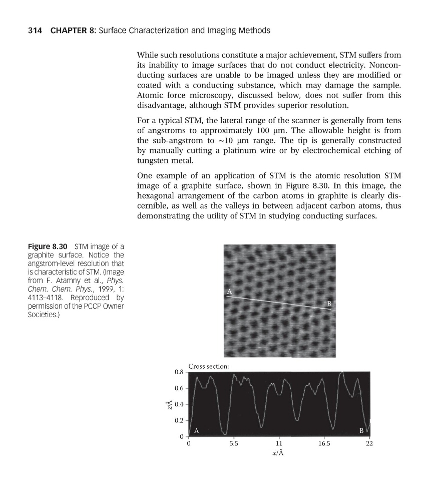
One example of an application of STM is the atomic resolution STM
image of a graphite surface, shown in Figure 8.30. In this image, the
hexagonal arrangement of the carbon atoms in graphite is clearly discernible, as well as the valleys in between adjacent carbon atoms, thus
demonstrating the utility of STM in studying conducting surfaces.
A
B
B
A
0
0
0.2
0.4
0.6
0.8
Cross section:
5.5
11
x/Å
z/Å
16.5
22
Figure 8.30 STM image of a
graphite surface. Notice the
angstrom-level resolution that
is characteristic of STM. (Image
from F. Atamny et al., Phys.
Chem. Chem. Phys., 1999, 1:
4113–4118. Reproduced by
permission of the PCCP Owner
Societies.)
CHAPTER 8: Surface Characterization and Imaging Methods
314
its inability to image surfaces that do not conduct electricity. Nonconducting surfaces are unable to be imaged unless they are modified or
coated with a conducting substance, which may damage the sample.
Atomic force microscopy, discussed below, does not suffer from this
disadvantage, although STM provides superior resolution.
For a typical STM, the lateral range of the scanner is generally from tens
of angstroms to approximately 100 µm. The allowable height is from
the sub-angstrom to ∼10 µm range. The tip is generally constructed
by manually cutting a platinum wire or by electrochemical etching of
tungsten metal.
One example of an application of STM is the atomic resolution STM
image of a graphite surface, shown in Figure 8.30. In this image, the
hexagonal arrangement of the carbon atoms in graphite is clearly discernible, as well as the valleys in between adjacent carbon atoms, thus
demonstrating the utility of STM in studying conducting surfaces.
A
B
B
A
0
0
0.2
0.4
0.6
0.8
Cross section:
5.5
11
x/Å
z/Å
16.5
22
Figure 8.30 STM image of a
graphite surface. Notice the
angstrom-level resolution that
is characteristic of STM. (Image
from F. Atamny et al., Phys.
Chem. Chem. Phys., 1999, 1:
4113–4118. Reproduced by
permission of the PCCP Owner
Societies.)
CHAPTER 8: Surface Characterization and Imaging Methods
314