

12.3 Electron Microscopy 287
specimens with particle sizes below ca. 140 nm, it is impossible to decide if the
specimen consists of the tetragonal, the cubic phase, or a mixture of both.
A very special technique for electron diffraction is the selected-area diffraction
(SAD), a technique that is already in transition to the local methods. In this case,
the electron beam is focused to a very small spot, enabling the operator to make
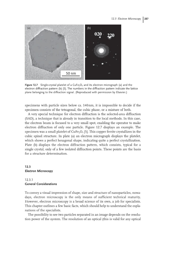
electron diffraction of only one particle. Figure 12.7 displays an example. The
specimen was a small platelet of CuFe 2 O 4 [5]. This copper ferrite crystallizes in the
cubic spinel structure. In plate (a) an electron micrograph displays the platelet,
which shows a perfect hexagonal shape, indicating quite a perfect crystallization.
Plate (b) displays the electron diffraction pattern, which consists, typical for a
single crystal, only of a few isolated diffraction points. These points are the basis
for a structure determination.
12.3
Electron Microscopy
12.3.1
General Considerations
To convey a visual impression of shape, size and structure of nanoparticles, nowadays, electron microscopy is the only means of sufficient technical maturity.
However, electron microscopy is a broad science of its own, a job for specialists.
This chapter outlines a few basic facts, which should help to understand the explanations of the specialists.
The possibility to see two particles separated in an image depends on the resolution power of the system. The resolution of an optical (this is valid for any optical
Figure 12.7 Single-crystal platelet of a CuFe 2 O 4 and its electron micrograph (a) and the
electron diffraction pattern (b) [5]. The numbers in the diffraction pattern indicate the lattice
plane belonging to the diffraction signal. (Reproduced with permission by Elsevier.)
50 nm
(a)
(b)
specimens with particle sizes below ca. 140 nm, it is impossible to decide if the
specimen consists of the tetragonal, the cubic phase, or a mixture of both.
A very special technique for electron diffraction is the selected-area diffraction
(SAD), a technique that is already in transition to the local methods. In this case,
the electron beam is focused to a very small spot, enabling the operator to make
electron diffraction of only one particle. Figure 12.7 displays an example. The
specimen was a small platelet of CuFe 2 O 4 [5]. This copper ferrite crystallizes in the
cubic spinel structure. In plate (a) an electron micrograph displays the platelet,
which shows a perfect hexagonal shape, indicating quite a perfect crystallization.
Plate (b) displays the electron diffraction pattern, which consists, typical for a
single crystal, only of a few isolated diffraction points. These points are the basis
for a structure determination.
12.3
Electron Microscopy
12.3.1
General Considerations
To convey a visual impression of shape, size and structure of nanoparticles, nowadays, electron microscopy is the only means of sufficient technical maturity.
However, electron microscopy is a broad science of its own, a job for specialists.
This chapter outlines a few basic facts, which should help to understand the explanations of the specialists.
The possibility to see two particles separated in an image depends on the resolution power of the system. The resolution of an optical (this is valid for any optical
Figure 12.7 Single-crystal platelet of a CuFe 2 O 4 and its electron micrograph (a) and the
electron diffraction pattern (b) [5]. The numbers in the diffraction pattern indicate the lattice
plane belonging to the diffraction signal. (Reproduced with permission by Elsevier.)
50 nm
(a)
(b)