

318
V. Melnik et al.
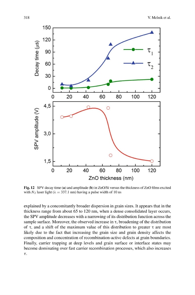
Fig. 12 SPV decay time (a) and amplitude (b) in ZnO/Si versus the thickness of ZnO films excited
with N 2 laser light (λ = 337.1 nm) having a pulse width of 10 ns
explained by a concomitantly broader dispersion in grain sizes. It appears that in the
thickness range from about 65 to 120 nm, when a dense consolidated layer occurs,
the SPV amplitude decreases with a narrowing of its distribution function across the
sample surface. Moreover, the observed increase in τ, broadening of the distribution
of τ, and a shift of the maximum value of this distribution to greater τ are most
likely due to the fact that increasing the grain size and grain density affects the
composition and concentration of recombination-active defects at grain boundaries.
Finally, carrier trapping at deep levels and grain surface or interface states may
become dominating over fast carrier recombination processes, which also increases
τ.
V. Melnik et al.
Fig. 12 SPV decay time (a) and amplitude (b) in ZnO/Si versus the thickness of ZnO films excited
with N 2 laser light (λ = 337.1 nm) having a pulse width of 10 ns
explained by a concomitantly broader dispersion in grain sizes. It appears that in the
thickness range from about 65 to 120 nm, when a dense consolidated layer occurs,
the SPV amplitude decreases with a narrowing of its distribution function across the
sample surface. Moreover, the observed increase in τ, broadening of the distribution
of τ, and a shift of the maximum value of this distribution to greater τ are most
likely due to the fact that increasing the grain size and grain density affects the
composition and concentration of recombination-active defects at grain boundaries.
Finally, carrier trapping at deep levels and grain surface or interface states may
become dominating over fast carrier recombination processes, which also increases
τ.