

Formation and Transient Photovoltaic Properties of ZnO/Si …
317
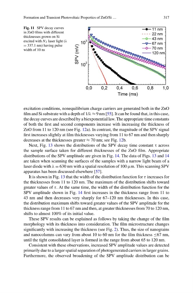
Fig. 11 SPV decay curves
in ZnO films with different
thicknesses grown on Si
excited with N 2 laser light (λ
= 337.1 nm) having pulse
width of 10 ns
excitation conditions, nonequilibrium charge carriers are generated both in the ZnO
film and Si substrate with a depth of 1/λ ≈ 9 nm [55]. It can be found that, in this case,
the decay curves are described by a biexponential law. The appropriate time constants
of both the first and second components increase with increasing the thickness of
ZnO from 11 to 120 nm (see Fig. 12a). In contrast, the magnitude of the SPV signal
first increases slightly at film thicknesses varying from 11 to 67 nm and then sharply
decreases at the thicknesses greater ≈ 70 nm; see Fig. 12b.
Next, Fig. 13 shows the distributions of the SPV decay time constant τ across
the sample surface taken for different thicknesses of the ZnO film. Appropriate
distributions of the SPV amplitude are given in Fig. 14. The data of Figs. 13 and 14
are taken when scanning the surfaces of the samples with a narrow light beam of a
laser diode with λ = 630 nm with a spatial resolution of 100 μm. This scanning SPV
apparatus has been discussed elsewhere [57].
It is shown in Fig. 13 that the width of the distribution function for τ increases for
the thicknesses from 11 to 120 nm. The maximum of the distribution shifts toward
greater values of τ. At the same time, the width of the distribution function for the
SPV amplitude shown in Fig. 14 first increases in the thickness range from 11 to
43 nm and then decreases very sharply for 67–120 nm thicknesses. In this case,
the distribution maximum shifts toward greater values of the SPV amplitude for the
thickness range from 11 to 67 nm and then, at greater thicknesses from 70 to 120 nm,
shifts to almost 100% of its initial value.
These SPV results can be explained as follows by taking the change of the film
morphology with its thickness into consideration. The film microstructure changes
significantly with increasing the thickness (see Fig. 2). Thus, the size of nanograins
and nanocolumns can vary from about 10 to 60 nm for the film thickness ≤67 nm,
until the tight consolidated layer is formed in the range from about 65 to 120 nm.
Consistent with these observations, increased SPV amplitude values are detected
primarily due to a larger spatial separation of photogenerated carriers in larger grains.
Furthermore, the observed broadening of the SPV amplitude distribution can be
317
Fig. 11 SPV decay curves
in ZnO films with different
thicknesses grown on Si
excited with N 2 laser light (λ
= 337.1 nm) having pulse
width of 10 ns
excitation conditions, nonequilibrium charge carriers are generated both in the ZnO
film and Si substrate with a depth of 1/λ ≈ 9 nm [55]. It can be found that, in this case,
the decay curves are described by a biexponential law. The appropriate time constants
of both the first and second components increase with increasing the thickness of
ZnO from 11 to 120 nm (see Fig. 12a). In contrast, the magnitude of the SPV signal
first increases slightly at film thicknesses varying from 11 to 67 nm and then sharply
decreases at the thicknesses greater ≈ 70 nm; see Fig. 12b.
Next, Fig. 13 shows the distributions of the SPV decay time constant τ across
the sample surface taken for different thicknesses of the ZnO film. Appropriate
distributions of the SPV amplitude are given in Fig. 14. The data of Figs. 13 and 14
are taken when scanning the surfaces of the samples with a narrow light beam of a
laser diode with λ = 630 nm with a spatial resolution of 100 μm. This scanning SPV
apparatus has been discussed elsewhere [57].
It is shown in Fig. 13 that the width of the distribution function for τ increases for
the thicknesses from 11 to 120 nm. The maximum of the distribution shifts toward
greater values of τ. At the same time, the width of the distribution function for the
SPV amplitude shown in Fig. 14 first increases in the thickness range from 11 to
43 nm and then decreases very sharply for 67–120 nm thicknesses. In this case,
the distribution maximum shifts toward greater values of the SPV amplitude for the
thickness range from 11 to 67 nm and then, at greater thicknesses from 70 to 120 nm,
shifts to almost 100% of its initial value.
These SPV results can be explained as follows by taking the change of the film
morphology with its thickness into consideration. The film microstructure changes
significantly with increasing the thickness (see Fig. 2). Thus, the size of nanograins
and nanocolumns can vary from about 10 to 60 nm for the film thickness ≤67 nm,
until the tight consolidated layer is formed in the range from about 65 to 120 nm.
Consistent with these observations, increased SPV amplitude values are detected
primarily due to a larger spatial separation of photogenerated carriers in larger grains.
Furthermore, the observed broadening of the SPV amplitude distribution can be