

10 Realization of Artificial Chirality in Micro-/Nano-Scale …
249
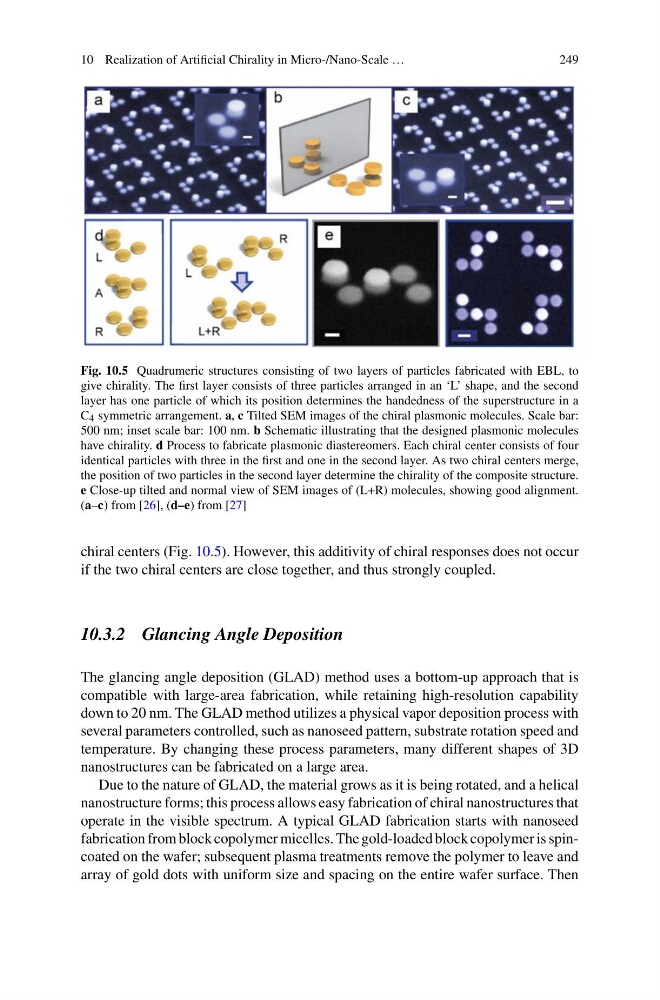
Fig. 10.5 Quadrumeric structures consisting of two layers of particles fabricated with EBL, to
give chirality. The first layer consists of three particles arranged in an ‘L’ shape, and the second
layer has one particle of which its position determines the handedness of the superstructure in a
C 4 symmetric arrangement. a, c Tilted SEM images of the chiral plasmonic molecules. Scale bar:
500 nm; inset scale bar: 100 nm. b Schematic illustrating that the designed plasmonic molecules
have chirality. d Process to fabricate plasmonic diastereomers. Each chiral center consists of four
identical particles with three in the first and one in the second layer. As two chiral centers merge,
the position of two particles in the second layer determine the chirality of the composite structure.
e Close-up tilted and normal view of SEM images of (L+R) molecules, showing good alignment.
(a–c) from [26], (d–e) from [27]
chiral centers (Fig. 10.5). However, this additivity of chiral responses does not occur
if the two chiral centers are close together, and thus strongly coupled.
10.3.2 Glancing Angle Deposition
The glancing angle deposition (GLAD) method uses a bottom-up approach that is
compatible with large-area fabrication, while retaining high-resolution capability
down to 20 nm. The GLAD method utilizes a physical vapor deposition process with
several parameters controlled, such as nanoseed pattern, substrate rotation speed and
temperature. By changing these process parameters, many different shapes of 3D
nanostructures can be fabricated on a large area.
Due to the nature of GLAD, the material grows as it is being rotated, and a helical
nanostructure forms; this process allows easy fabrication of chiral nanostructures that
operate in the visible spectrum. A typical GLAD fabrication starts with nanoseed
fabrication from block copolymer micelles. The gold-loaded block copolymer is spincoated on the wafer; subsequent plasma treatments remove the polymer to leave and
array of gold dots with uniform size and spacing on the entire wafer surface. Then
249
Fig. 10.5 Quadrumeric structures consisting of two layers of particles fabricated with EBL, to
give chirality. The first layer consists of three particles arranged in an ‘L’ shape, and the second
layer has one particle of which its position determines the handedness of the superstructure in a
C 4 symmetric arrangement. a, c Tilted SEM images of the chiral plasmonic molecules. Scale bar:
500 nm; inset scale bar: 100 nm. b Schematic illustrating that the designed plasmonic molecules
have chirality. d Process to fabricate plasmonic diastereomers. Each chiral center consists of four
identical particles with three in the first and one in the second layer. As two chiral centers merge,
the position of two particles in the second layer determine the chirality of the composite structure.
e Close-up tilted and normal view of SEM images of (L+R) molecules, showing good alignment.
(a–c) from [26], (d–e) from [27]
chiral centers (Fig. 10.5). However, this additivity of chiral responses does not occur
if the two chiral centers are close together, and thus strongly coupled.
10.3.2 Glancing Angle Deposition
The glancing angle deposition (GLAD) method uses a bottom-up approach that is
compatible with large-area fabrication, while retaining high-resolution capability
down to 20 nm. The GLAD method utilizes a physical vapor deposition process with
several parameters controlled, such as nanoseed pattern, substrate rotation speed and
temperature. By changing these process parameters, many different shapes of 3D
nanostructures can be fabricated on a large area.
Due to the nature of GLAD, the material grows as it is being rotated, and a helical
nanostructure forms; this process allows easy fabrication of chiral nanostructures that
operate in the visible spectrum. A typical GLAD fabrication starts with nanoseed
fabrication from block copolymer micelles. The gold-loaded block copolymer is spincoated on the wafer; subsequent plasma treatments remove the polymer to leave and
array of gold dots with uniform size and spacing on the entire wafer surface. Then