

138
A. P. Pyatakov et al.
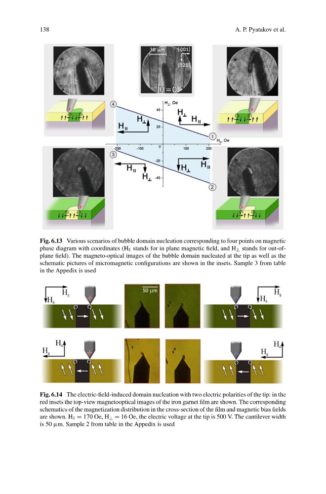
Fig. 6.13 Various scenarios of bubble domain nucleation corresponding to four points on magnetic
phase diagram with coordinates (H stands for in plane magnetic field, and H ⊥ stands for out-ofplane field). The magneto-optical images of the bubble domain nucleated at the tip as well as the
schematic pictures of micromagnetic configurations are shown in the insets. Sample 3 from table
in the Appedix is used
Fig. 6.14 The electric-field-induced domain nucleation with two electric polarities of the tip: in the
red insets the top-view magnetooptical images of the iron garnet film are shown. The corresponding
schematics of the magnetization distribution in the cross-section of the film and magnetic bias fields
are shown. H = 170 Oe, H ⊥ = 16 Oe, the electric voltage at the tip is 500 V. The cantilever width
is 50 μm. Sample 2 from table in the Appedix is used
A. P. Pyatakov et al.
Fig. 6.13 Various scenarios of bubble domain nucleation corresponding to four points on magnetic
phase diagram with coordinates (H stands for in plane magnetic field, and H ⊥ stands for out-ofplane field). The magneto-optical images of the bubble domain nucleated at the tip as well as the
schematic pictures of micromagnetic configurations are shown in the insets. Sample 3 from table
in the Appedix is used
Fig. 6.14 The electric-field-induced domain nucleation with two electric polarities of the tip: in the
red insets the top-view magnetooptical images of the iron garnet film are shown. The corresponding
schematics of the magnetization distribution in the cross-section of the film and magnetic bias fields
are shown. H = 170 Oe, H ⊥ = 16 Oe, the electric voltage at the tip is 500 V. The cantilever width
is 50 μm. Sample 2 from table in the Appedix is used