

4 Chirality and Antiferromagnetism in Optical Metasurfaces
89
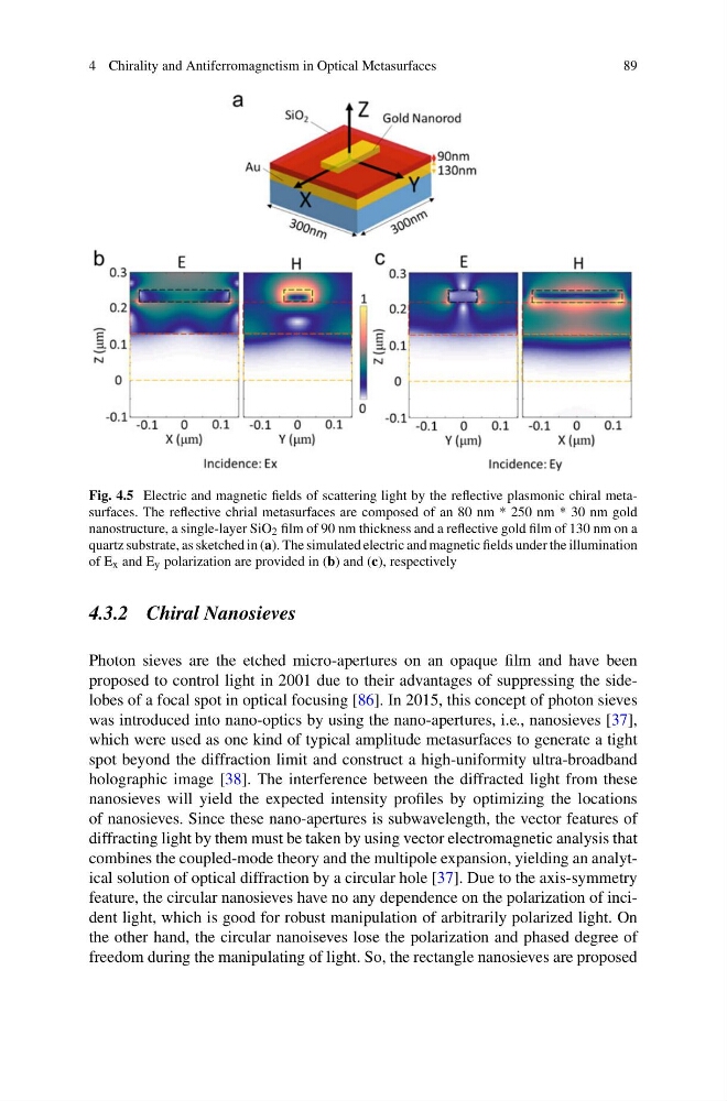
Fig. 4.5 Electric and magnetic fields of scattering light by the reflective plasmonic chiral metasurfaces. The reflective chrial metasurfaces are composed of an 80 nm * 250 nm * 30 nm gold
nanostructure, a single-layer SiO 2 film of 90 nm thickness and a reflective gold film of 130 nm on a
quartz substrate, as sketched in (a). The simulated electric and magnetic fields under the illumination
of E x and E y polarization are provided in (b) and (c), respectively
4.3.2 Chiral Nanosieves
Photon sieves are the etched micro-apertures on an opaque film and have been
proposed to control light in 2001 due to their advantages of suppressing the sidelobes of a focal spot in optical focusing [86]. In 2015, this concept of photon sieves
was introduced into nano-optics by using the nano-apertures, i.e., nanosieves [37],
which were used as one kind of typical amplitude metasurfaces to generate a tight
spot beyond the diffraction limit and construct a high-uniformity ultra-broadband
holographic image [38]. The interference between the diffracted light from these
nanosieves will yield the expected intensity profiles by optimizing the locations
of nanosieves. Since these nano-apertures is subwavelength, the vector features of
diffracting light by them must be taken by using vector electromagnetic analysis that
combines the coupled-mode theory and the multipole expansion, yielding an analytical solution of optical diffraction by a circular hole [37]. Due to the axis-symmetry
feature, the circular nanosieves have no any dependence on the polarization of incident light, which is good for robust manipulation of arbitrarily polarized light. On
the other hand, the circular nanoiseves lose the polarization and phased degree of
freedom during the manipulating of light. So, the rectangle nanosieves are proposed
89
Fig. 4.5 Electric and magnetic fields of scattering light by the reflective plasmonic chiral metasurfaces. The reflective chrial metasurfaces are composed of an 80 nm * 250 nm * 30 nm gold
nanostructure, a single-layer SiO 2 film of 90 nm thickness and a reflective gold film of 130 nm on a
quartz substrate, as sketched in (a). The simulated electric and magnetic fields under the illumination
of E x and E y polarization are provided in (b) and (c), respectively
4.3.2 Chiral Nanosieves
Photon sieves are the etched micro-apertures on an opaque film and have been
proposed to control light in 2001 due to their advantages of suppressing the sidelobes of a focal spot in optical focusing [86]. In 2015, this concept of photon sieves
was introduced into nano-optics by using the nano-apertures, i.e., nanosieves [37],
which were used as one kind of typical amplitude metasurfaces to generate a tight
spot beyond the diffraction limit and construct a high-uniformity ultra-broadband
holographic image [38]. The interference between the diffracted light from these
nanosieves will yield the expected intensity profiles by optimizing the locations
of nanosieves. Since these nano-apertures is subwavelength, the vector features of
diffracting light by them must be taken by using vector electromagnetic analysis that
combines the coupled-mode theory and the multipole expansion, yielding an analytical solution of optical diffraction by a circular hole [37]. Due to the axis-symmetry
feature, the circular nanosieves have no any dependence on the polarization of incident light, which is good for robust manipulation of arbitrarily polarized light. On
the other hand, the circular nanoiseves lose the polarization and phased degree of
freedom during the manipulating of light. So, the rectangle nanosieves are proposed