

chapter 8 nanomaterials: Synthesis and characterization
282
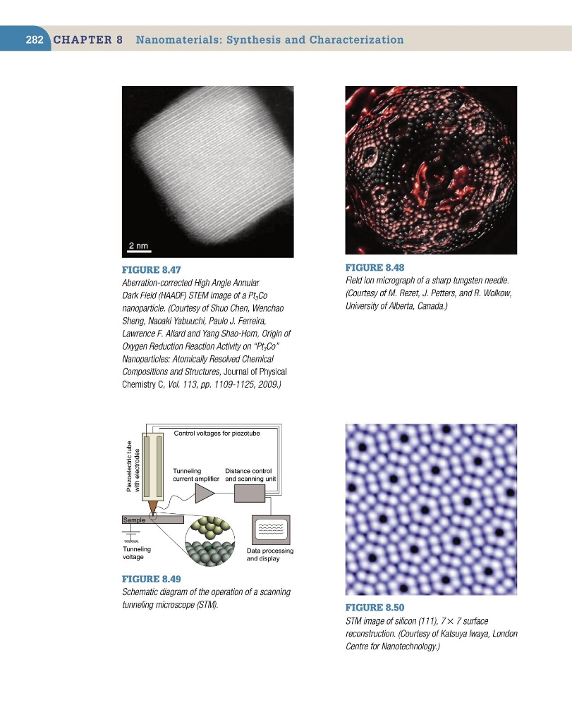
Figure 8.47
Aberration-corrected High Angle Annular
Dark Field (HAADF) STEM image of a Pt 3 Co
nanoparticle. (Courtesy of Shuo Chen, Wenchao
Sheng, Naoaki Yabuuchi, Paulo J. Ferreira,
Lawrence F. Allard and Yang Shao-Horn, Origin of
Oxygen Reduction Reaction Activity on “Pt 3 Co”
Nanoparticles: Atomically Resolved Chemical
Compositions and Structures, Journal of Physical
Chemistry C, Vol. 113, pp. 1109-1125, 2009.)
Figure 8.48
Field ion micrograph of a sharp tungsten needle.
(Courtesy of M. Rezet, J. Petters, and R. Wolkow,
University of Alberta, Canada.)
Figure 8.49
Schematic diagram of the operation of a scanning
tunneling microscope (STM).
Distance control
and scanning unit
Tunneling
current amplifier
Data processing
and display
Tunneling
voltage
Control voltages for piezotube
Piezoelectric tube
with electrodes
Sample
Figure 8.50
STM image of silicon (111), 7 × 7 surface
reconstruction. (Courtesy of Katsuya Iwaya, London
Centre for Nanotechnology.)
282
Figure 8.47
Aberration-corrected High Angle Annular
Dark Field (HAADF) STEM image of a Pt 3 Co
nanoparticle. (Courtesy of Shuo Chen, Wenchao
Sheng, Naoaki Yabuuchi, Paulo J. Ferreira,
Lawrence F. Allard and Yang Shao-Horn, Origin of
Oxygen Reduction Reaction Activity on “Pt 3 Co”
Nanoparticles: Atomically Resolved Chemical
Compositions and Structures, Journal of Physical
Chemistry C, Vol. 113, pp. 1109-1125, 2009.)
Figure 8.48
Field ion micrograph of a sharp tungsten needle.
(Courtesy of M. Rezet, J. Petters, and R. Wolkow,
University of Alberta, Canada.)
Figure 8.49
Schematic diagram of the operation of a scanning
tunneling microscope (STM).
Distance control
and scanning unit
Tunneling
current amplifier
Data processing
and display
Tunneling
voltage
Control voltages for piezotube
Piezoelectric tube
with electrodes
Sample
Figure 8.50
STM image of silicon (111), 7 × 7 surface
reconstruction. (Courtesy of Katsuya Iwaya, London
Centre for Nanotechnology.)