

281
gation of elements as well as atomic variations in composition in
nanostructures.
Another instrumental technique in which the resolution is on
the order of interatomic dimensions is field ion microscopy
(FIM). Instead of electrons, this method uses ions. In FIM, a sharp
(between 5 nm and 50 nm tip radius) metal tip is prepared and
placed in an ultra-high-vacuum chamber under cryogenic temperatures (20–100°K). The chamber is backfilled with an imaging inert
gas such as helium or neon, and a positive voltage (between 5 kV
and 20 kV) is held at the tip. The gas atoms adsorbed on the tip are
positively ionized by the electric field, repelled from the tip, and
accelerated toward a fluorescent screen, where they create spots (see
Figure 8.48).
In principle, each spot on the fluorescent screen corresponds to an
atom on the tip so that the distribution of spots on the image represents the atomic configuration on the tip. The image magnification
is given by the ratio between the radius of the screen and the radius
of the tip, which is typically a few million times. Unlike conventional microscopes, where the spatial resolution is limited by the
wavelength of the particles that are used for imaging, the FIM is a
projection type microscope with atomic resolution. The major disadvantages of this technique are the fabrication and contamination
of the tip as well as the relatively small number of materials that
resist evaporation during the ionization of the inert gas atoms.
Finally, we are left with those techniques for imaging using a scanning probe. Two methods are highly used for the study of nanomaterials and nanotechnologies: the scanning tunneling microscope
(STM) and the atomic force microscope (AFM). The STM technique
allows the real space imaging of electrically conductive surfaces
down to the atomic scale. The method uses a very sharp conducting tip with a bias voltage applied between the tip and the sample.
The tip is mechanically connected to a scanner, which is a threedimensional positioning device driven by piezoelectric actuators.
Under these conditions, the tip can be laterally moved to scan the
sample surface; changing the vertical position allows one to maintain a desired distance between the tip and the sample (see Figure
8.49). When the tip is brought within about 1 nm of the sample
surface, the electron wave functions of the tip and sample overlap,
causing electrons to tunnel across the gap and produce a current.
It is this current that is used to form an STM image (see Figure
8.50). Because the tunneling current is exponentially dependent on the tip-sample distance, small variations in distance lead
Characterization of Nanomaterials
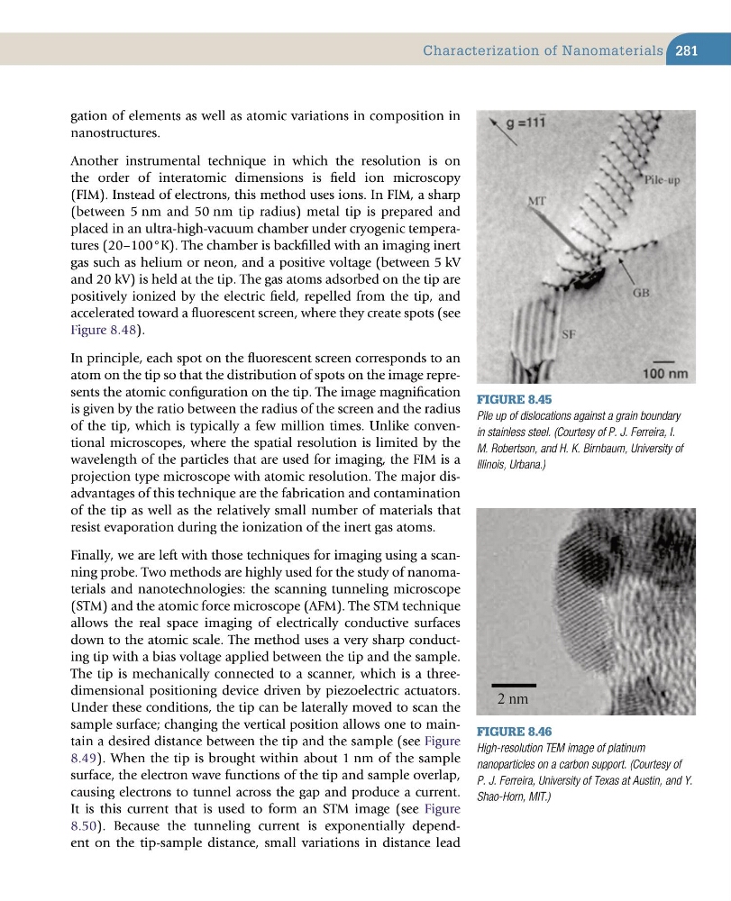
Figure 8.45
Pile up of dislocations against a grain boundary
in stainless steel. (Courtesy of P. J. Ferreira, I.
M. Robertson, and H. K. Birnbaum, University of
Illinois, Urbana.)
Figure 8.46
High-resolution TEM image of platinum
nanoparticles on a carbon support. (Courtesy of
P. J. Ferreira, University of Texas at Austin, and Y.
Shao-Horn, MIT.)
gation of elements as well as atomic variations in composition in
nanostructures.
Another instrumental technique in which the resolution is on
the order of interatomic dimensions is field ion microscopy
(FIM). Instead of electrons, this method uses ions. In FIM, a sharp
(between 5 nm and 50 nm tip radius) metal tip is prepared and
placed in an ultra-high-vacuum chamber under cryogenic temperatures (20–100°K). The chamber is backfilled with an imaging inert
gas such as helium or neon, and a positive voltage (between 5 kV
and 20 kV) is held at the tip. The gas atoms adsorbed on the tip are
positively ionized by the electric field, repelled from the tip, and
accelerated toward a fluorescent screen, where they create spots (see
Figure 8.48).
In principle, each spot on the fluorescent screen corresponds to an
atom on the tip so that the distribution of spots on the image represents the atomic configuration on the tip. The image magnification
is given by the ratio between the radius of the screen and the radius
of the tip, which is typically a few million times. Unlike conventional microscopes, where the spatial resolution is limited by the
wavelength of the particles that are used for imaging, the FIM is a
projection type microscope with atomic resolution. The major disadvantages of this technique are the fabrication and contamination
of the tip as well as the relatively small number of materials that
resist evaporation during the ionization of the inert gas atoms.
Finally, we are left with those techniques for imaging using a scanning probe. Two methods are highly used for the study of nanomaterials and nanotechnologies: the scanning tunneling microscope
(STM) and the atomic force microscope (AFM). The STM technique
allows the real space imaging of electrically conductive surfaces
down to the atomic scale. The method uses a very sharp conducting tip with a bias voltage applied between the tip and the sample.
The tip is mechanically connected to a scanner, which is a threedimensional positioning device driven by piezoelectric actuators.
Under these conditions, the tip can be laterally moved to scan the
sample surface; changing the vertical position allows one to maintain a desired distance between the tip and the sample (see Figure
8.49). When the tip is brought within about 1 nm of the sample
surface, the electron wave functions of the tip and sample overlap,
causing electrons to tunnel across the gap and produce a current.
It is this current that is used to form an STM image (see Figure
8.50). Because the tunneling current is exponentially dependent on the tip-sample distance, small variations in distance lead
Characterization of Nanomaterials
Figure 8.45
Pile up of dislocations against a grain boundary
in stainless steel. (Courtesy of P. J. Ferreira, I.
M. Robertson, and H. K. Birnbaum, University of
Illinois, Urbana.)
Figure 8.46
High-resolution TEM image of platinum
nanoparticles on a carbon support. (Courtesy of
P. J. Ferreira, University of Texas at Austin, and Y.
Shao-Horn, MIT.)