

chapter 8 nanomaterials: Synthesis and characterization
280
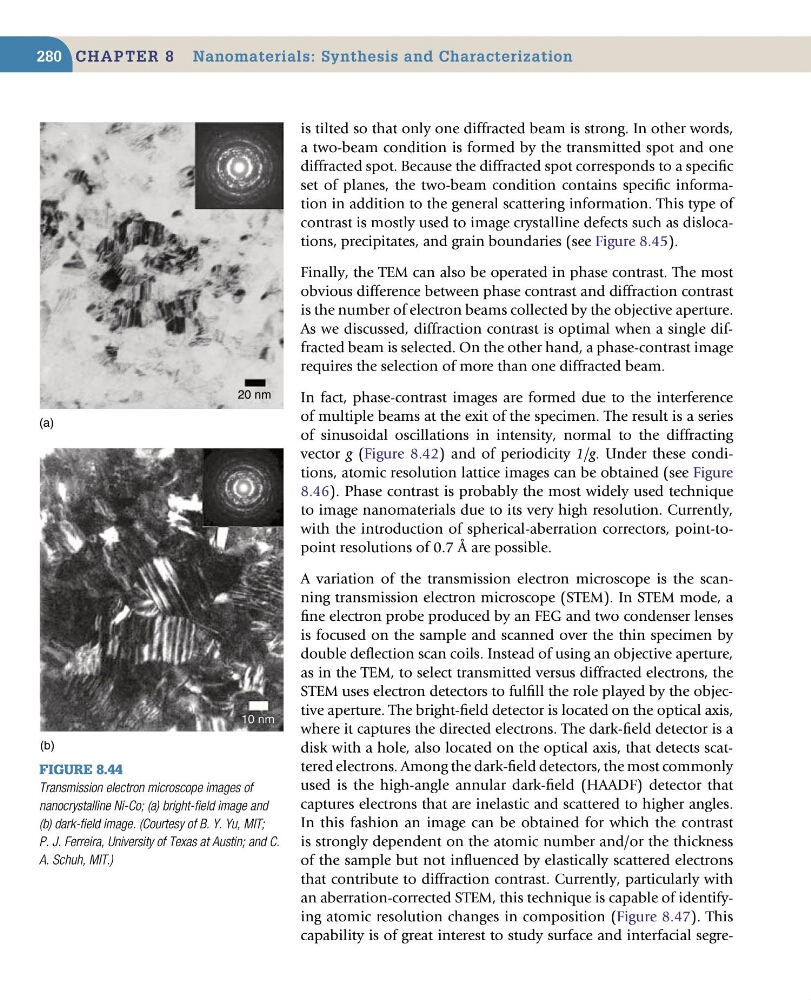
Figure 8.44
Transmission electron microscope images of
nanocrystalline Ni-Co; (a) bright-field image and
(b) dark-field image. (Courtesy of B. Y. Yu, MIT;
P. J. Ferreira, University of Texas at Austin; and C.
A. Schuh, MIT.)
(a)
(b)
20 nm
10 nm
is tilted so that only one diffracted beam is strong. In other words,
a two-beam condition is formed by the transmitted spot and one
diffracted spot. Because the diffracted spot corresponds to a specific
set of planes, the two-beam condition contains specific information in addition to the general scattering information. This type of
contrast is mostly used to image crystalline defects such as dislocations, precipitates, and grain boundaries (see Figure 8.45).
Finally, the TEM can also be operated in phase contrast. The most
obvious difference between phase contrast and diffraction contrast
is the number of electron beams collected by the objective aperture.
As we discussed, diffraction contrast is optimal when a single diffracted beam is selected. On the other hand, a phase-contrast image
requires the selection of more than one diffracted beam.
In fact, phase-contrast images are formed due to the interference
of multiple beams at the exit of the specimen. The result is a series
of sinusoidal oscillations in intensity, normal to the diffracting
vector g (Figure 8.42) and of periodicity 1/g. Under these conditions, atomic resolution lattice images can be obtained (see Figure
8.46). Phase contrast is probably the most widely used technique
to image nanomaterials due to its very high resolution. Currently,
with the introduction of spherical-aberration correctors, point-topoint resolutions of 0.7 Å are possible.
A variation of the transmission electron microscope is the scanning transmission electron microscope (STEM). In STEM mode, a
fine electron probe produced by an FEG and two condenser lenses
is focused on the sample and scanned over the thin specimen by
double deflection scan coils. Instead of using an objective aperture,
as in the TEM, to select transmitted versus diffracted electrons, the
STEM uses electron detectors to fulfill the role played by the objective aperture. The bright-field detector is located on the optical axis,
where it captures the directed electrons. The dark-field detector is a
disk with a hole, also located on the optical axis, that detects scattered electrons. Among the dark-field detectors, the most commonly
used is the high-angle annular dark-field (HAADF) detector that
captures electrons that are inelastic and scattered to higher angles.
In this fashion an image can be obtained for which the contrast
is strongly dependent on the atomic number and/or the thickness
of the sample but not influenced by elastically scattered electrons
that contribute to diffraction contrast. Currently, particularly with
an aberration-corrected STEM, this technique is capable of identifying atomic resolution changes in composition (Figure 8.47). This
capability is of great interest to study surface and interfacial segre-
280
Figure 8.44
Transmission electron microscope images of
nanocrystalline Ni-Co; (a) bright-field image and
(b) dark-field image. (Courtesy of B. Y. Yu, MIT;
P. J. Ferreira, University of Texas at Austin; and C.
A. Schuh, MIT.)
(a)
(b)
20 nm
10 nm
is tilted so that only one diffracted beam is strong. In other words,
a two-beam condition is formed by the transmitted spot and one
diffracted spot. Because the diffracted spot corresponds to a specific
set of planes, the two-beam condition contains specific information in addition to the general scattering information. This type of
contrast is mostly used to image crystalline defects such as dislocations, precipitates, and grain boundaries (see Figure 8.45).
Finally, the TEM can also be operated in phase contrast. The most
obvious difference between phase contrast and diffraction contrast
is the number of electron beams collected by the objective aperture.
As we discussed, diffraction contrast is optimal when a single diffracted beam is selected. On the other hand, a phase-contrast image
requires the selection of more than one diffracted beam.
In fact, phase-contrast images are formed due to the interference
of multiple beams at the exit of the specimen. The result is a series
of sinusoidal oscillations in intensity, normal to the diffracting
vector g (Figure 8.42) and of periodicity 1/g. Under these conditions, atomic resolution lattice images can be obtained (see Figure
8.46). Phase contrast is probably the most widely used technique
to image nanomaterials due to its very high resolution. Currently,
with the introduction of spherical-aberration correctors, point-topoint resolutions of 0.7 Å are possible.
A variation of the transmission electron microscope is the scanning transmission electron microscope (STEM). In STEM mode, a
fine electron probe produced by an FEG and two condenser lenses
is focused on the sample and scanned over the thin specimen by
double deflection scan coils. Instead of using an objective aperture,
as in the TEM, to select transmitted versus diffracted electrons, the
STEM uses electron detectors to fulfill the role played by the objective aperture. The bright-field detector is located on the optical axis,
where it captures the directed electrons. The dark-field detector is a
disk with a hole, also located on the optical axis, that detects scattered electrons. Among the dark-field detectors, the most commonly
used is the high-angle annular dark-field (HAADF) detector that
captures electrons that are inelastic and scattered to higher angles.
In this fashion an image can be obtained for which the contrast
is strongly dependent on the atomic number and/or the thickness
of the sample but not influenced by elastically scattered electrons
that contribute to diffraction contrast. Currently, particularly with
an aberration-corrected STEM, this technique is capable of identifying atomic resolution changes in composition (Figure 8.47). This
capability is of great interest to study surface and interfacial segre-