

279
vector from the center spot T to an hkl spot is called a g hkl vector.
A g hkl vector is aligned perpendicular to the orientation of the hkl
plane, which runs parallel to the electron beam.
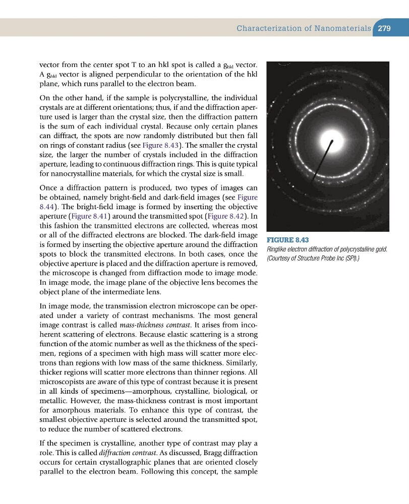
On the other hand, if the sample is polycrystalline, the individual
crystals are at different orientations; thus, if and the diffraction aperture used is larger than the crystal size, then the diffraction pattern
is the sum of each individual crystal. Because only certain planes
can diffract, the spots are now randomly distributed but then fall
on rings of constant radius (see Figure 8.43). The smaller the crystal
size, the larger the number of crystals included in the diffraction
aperture, leading to continuous diffraction rings. This is quite typical
for nanocrystalline materials, for which the crystal size is small.
Once a diffraction pattern is produced, two types of images can
be obtained, namely bright-field and dark-field images (see Figure
8.44). The bright-field image is formed by inserting the objective
aperture (Figure 8.41) around the transmitted spot (Figure 8.42). In
this fashion the transmitted electrons are collected, whereas most
or all of the diffracted electrons are blocked. The dark-field image
is formed by inserting the objective aperture around the diffraction
spots to block the transmitted electrons. In both cases, once the
objective aperture is placed and the diffraction aperture is removed,
the microscope is changed from diffraction mode to image mode.
In image mode, the image plane of the objective lens becomes the
object plane of the intermediate lens.
In image mode, the transmission electron microscope can be operated under a variety of contrast mechanisms. The most general
image contrast is called mass-thickness contrast. It arises from incoherent scattering of electrons. Because elastic scattering is a strong
function of the atomic number as well as the thickness of the specimen, regions of a specimen with high mass will scatter more electrons than regions with low mass of the same thickness. Similarly,
thicker regions will scatter more electrons than thinner regions. All
microscopists are aware of this type of contrast because it is present
in all kinds of specimens—amorphous, crystalline, biological, or
metallic. However, the mass-thickness contrast is most important
for amorphous materials. To enhance this type of contrast, the
smallest objective aperture is selected around the transmitted spot,
to reduce the number of scattered electrons.
If the specimen is crystalline, another type of contrast may play a
role. This is called diffraction contrast. As discussed, Bragg diffraction
occurs for certain crystallographic planes that are oriented closely
parallel to the electron beam. Following this concept, the sample
Characterization of Nanomaterials
Figure 8.43
Ringlike electron diffraction of polycrystalline gold.
(Courtesy of Structure Probe Inc (SPI).)
vector from the center spot T to an hkl spot is called a g hkl vector.
A g hkl vector is aligned perpendicular to the orientation of the hkl
plane, which runs parallel to the electron beam.
On the other hand, if the sample is polycrystalline, the individual
crystals are at different orientations; thus, if and the diffraction aperture used is larger than the crystal size, then the diffraction pattern
is the sum of each individual crystal. Because only certain planes
can diffract, the spots are now randomly distributed but then fall
on rings of constant radius (see Figure 8.43). The smaller the crystal
size, the larger the number of crystals included in the diffraction
aperture, leading to continuous diffraction rings. This is quite typical
for nanocrystalline materials, for which the crystal size is small.
Once a diffraction pattern is produced, two types of images can
be obtained, namely bright-field and dark-field images (see Figure
8.44). The bright-field image is formed by inserting the objective
aperture (Figure 8.41) around the transmitted spot (Figure 8.42). In
this fashion the transmitted electrons are collected, whereas most
or all of the diffracted electrons are blocked. The dark-field image
is formed by inserting the objective aperture around the diffraction
spots to block the transmitted electrons. In both cases, once the
objective aperture is placed and the diffraction aperture is removed,
the microscope is changed from diffraction mode to image mode.
In image mode, the image plane of the objective lens becomes the
object plane of the intermediate lens.
In image mode, the transmission electron microscope can be operated under a variety of contrast mechanisms. The most general
image contrast is called mass-thickness contrast. It arises from incoherent scattering of electrons. Because elastic scattering is a strong
function of the atomic number as well as the thickness of the specimen, regions of a specimen with high mass will scatter more electrons than regions with low mass of the same thickness. Similarly,
thicker regions will scatter more electrons than thinner regions. All
microscopists are aware of this type of contrast because it is present
in all kinds of specimens—amorphous, crystalline, biological, or
metallic. However, the mass-thickness contrast is most important
for amorphous materials. To enhance this type of contrast, the
smallest objective aperture is selected around the transmitted spot,
to reduce the number of scattered electrons.
If the specimen is crystalline, another type of contrast may play a
role. This is called diffraction contrast. As discussed, Bragg diffraction
occurs for certain crystallographic planes that are oriented closely
parallel to the electron beam. Following this concept, the sample
Characterization of Nanomaterials
Figure 8.43
Ringlike electron diffraction of polycrystalline gold.
(Courtesy of Structure Probe Inc (SPI).)