

chapter 8 nanomaterials: Synthesis and characterization
278
specimen and controls the spot size. Just below the second condenser lens is a condenser aperture that can be used to change the
electron current and therefore the intensity of the beam as well as
change the angle of beam convergence, which modifies the coherence of the beam. The specimen sits below the condenser lens and
above the objective lens. The specimen position and the objective
lens are the heart of the TEM, whereas the combination of the objective lens, the intermediate lens, and the projection lens determine
the overall magnification of the microscope.
In general, the TEM can be operated in image mode versus diffraction mode. The first mode to master is diffraction mode. It is here
that the electrons are selected to form the images. To obtain the diffraction pattern on the screen, the lens needs to be adjusted so that
the back focal plane of the objective lens acts as the object plane of
the intermediate lens. However, if we produce a diffraction pattern
by allowing all electrons to reach the screen, the high intensity of
the beam can damage the viewing screen and the information. In
addition, the gathered information is not very useful, because it
arises from all the area of observation.
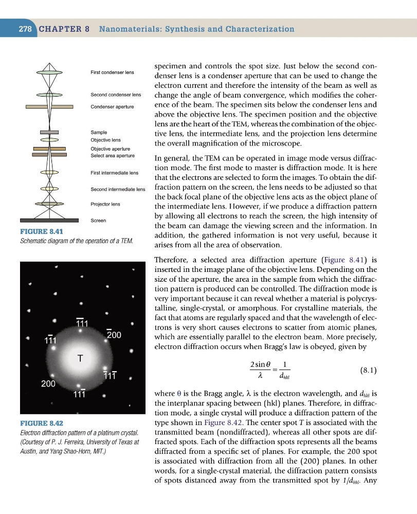
Therefore, a selected area diffraction aperture (Figure 8.41) is
inserted in the image plane of the objective lens. Depending on the
size of the aperture, the area in the sample from which the diffraction pattern is produced can be controlled. The diffraction mode is
very important because it can reveal whether a material is polycrystalline, single-crystal, or amorphous. For crystalline materials, the
fact that atoms are regularly spaced and that the wavelength of electrons is very short causes electrons to scatter from atomic planes,
which are essentially parallel to the electron beam. More precisely,
electron diffraction occurs when Bragg’s law is obeyed, given by
2
1
sinθ
λ
= d hkl
(8.1)
where θ is the Bragg angle, λ is the electron wavelength, and d hkl is
the interplanar spacing between (hkl) planes. Therefore, in diffraction mode, a single crystal will produce a diffraction pattern of the
type shown in Figure 8.42. The center spot T is associated with the
transmitted beam (nondiffracted), whereas all other spots are diffracted spots. Each of the diffraction spots represents all the beams
diffracted from a specific set of planes. For example, the 200 spot
is associated with diffraction from all the (200) planes. In other
words, for a single-crystal material, the diffraction pattern consists
of spots distanced away from the transmitted spot by 1/d hkl . Any
Figure 8.41
Schematic diagram of the operation of a TEM.
First condenser lens
Screen
Projector lens
Second intermediate lens
First intermediate lens
Select area aperture
Objective aperture
Objective lens
Sample
Condenser aperture
Second condenser lens
Figure 8.42
Electron diffraction pattern of a platinum crystal.
(Courtesy of P. J. Ferreira, University of Texas at
Austin, and Yang Shao-Horn, MIT.)
278
specimen and controls the spot size. Just below the second condenser lens is a condenser aperture that can be used to change the
electron current and therefore the intensity of the beam as well as
change the angle of beam convergence, which modifies the coherence of the beam. The specimen sits below the condenser lens and
above the objective lens. The specimen position and the objective
lens are the heart of the TEM, whereas the combination of the objective lens, the intermediate lens, and the projection lens determine
the overall magnification of the microscope.
In general, the TEM can be operated in image mode versus diffraction mode. The first mode to master is diffraction mode. It is here
that the electrons are selected to form the images. To obtain the diffraction pattern on the screen, the lens needs to be adjusted so that
the back focal plane of the objective lens acts as the object plane of
the intermediate lens. However, if we produce a diffraction pattern
by allowing all electrons to reach the screen, the high intensity of
the beam can damage the viewing screen and the information. In
addition, the gathered information is not very useful, because it
arises from all the area of observation.
Therefore, a selected area diffraction aperture (Figure 8.41) is
inserted in the image plane of the objective lens. Depending on the
size of the aperture, the area in the sample from which the diffraction pattern is produced can be controlled. The diffraction mode is
very important because it can reveal whether a material is polycrystalline, single-crystal, or amorphous. For crystalline materials, the
fact that atoms are regularly spaced and that the wavelength of electrons is very short causes electrons to scatter from atomic planes,
which are essentially parallel to the electron beam. More precisely,
electron diffraction occurs when Bragg’s law is obeyed, given by
2
1
sinθ
λ
= d hkl
(8.1)
where θ is the Bragg angle, λ is the electron wavelength, and d hkl is
the interplanar spacing between (hkl) planes. Therefore, in diffraction mode, a single crystal will produce a diffraction pattern of the
type shown in Figure 8.42. The center spot T is associated with the
transmitted beam (nondiffracted), whereas all other spots are diffracted spots. Each of the diffraction spots represents all the beams
diffracted from a specific set of planes. For example, the 200 spot
is associated with diffraction from all the (200) planes. In other
words, for a single-crystal material, the diffraction pattern consists
of spots distanced away from the transmitted spot by 1/d hkl . Any
Figure 8.41
Schematic diagram of the operation of a TEM.
First condenser lens
Screen
Projector lens
Second intermediate lens
First intermediate lens
Select area aperture
Objective aperture
Objective lens
Sample
Condenser aperture
Second condenser lens
Figure 8.42
Electron diffraction pattern of a platinum crystal.
(Courtesy of P. J. Ferreira, University of Texas at
Austin, and Yang Shao-Horn, MIT.)