

chapter 8 nanomaterials: Synthesis and characterization
276
avoid electron charging and image degradation. The basic layout
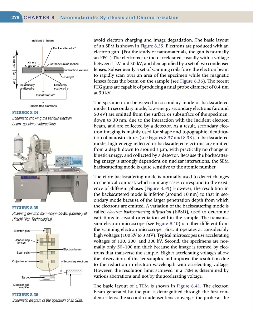
of an SEM is shown in Figure 8.35. Electrons are produced with an
electron gun. (For the study of nanomaterials, the gun is normally
an FEG.) The electrons are then accelerated, usually with a voltage
between 1 kV and 30 kV, and demagnified by a set of two condenser
lenses. Subsequently a set of scanning coils force the electron beam
to rapidly scan over an area of the specimen while the magnetic
lenses focus the beam on the sample (see Figure 8.36). The recent
FEG guns are capable of producing a final probe diameter of 0.4 nm
at 30 kV.
The specimen can be viewed in secondary mode or backscattered
mode. In secondary mode, low-energy secondary electrons (around
50 eV) are emitted from the surface or subsurface of the specimen,
down to 30 nm, due to the interaction with the incident electron
beam, and are collected by a detector. As a result, secondary electron imaging is mainly used for shape and topographic identification of nanostructures (see Figures 8.37 and 8.38). In backscattered
mode, high-energy reflected or backscattered electrons are emitted
from a depth down to around 1 µm, with practically no change in
kinetic energy, and collected by a detector. Because the backscattering energy is strongly dependent on nuclear interactions, the SEM
backscattering mode is quite sensitive to the atomic number.
Therefore backscattering mode is normally used to detect changes
in chemical contrast, which in many cases correspond to the existence of different phases (Figure 8.39) However, the resolution in
the backscattered mode is inferior (around 10 nm) to that in secondary mode because of the larger penetration depth from which
the electrons are emitted. A variation of the backscattering mode is
called electron backscattering diffraction (EBSD), used to determine
variations in crystal orientation within the sample. The transmission electron microscope (see Figure 8.40) is rather different from
the scanning electron microscope. First, it operates at considerably
high voltages (100 kV to 3 MV). Typical microscopes use accelerating
voltages of 120, 200, and 300 kV. Second, the specimens are normally only 50–100 nm thick because the image is formed by electrons that transverse the sample. Higher accelerating voltages allow
the observation of thicker samples and improve the resolution due
to the reduction in electron wavelength with accelerating voltage.
However, the resolution limit achieved in a TEM is determined by
various aberrations and not by the accelerating voltage.
The basic layout of a TEM is shown in Figure 8.41. The electron
beam generated by the gun is demagnified through the first condenser lens; the second condenser lens converges the probe at the
Figure 8.34
Schematic showing the various electron
beam–specimen interactions.
Fall (TEM) Bulk (SEM)
Backscattered e –
Cathodeluminescence
Auger e –
X-rays
Elastically
scattered e –
Inelastically
scattered e –
Unscattered e –
Sample
Interaction volume
Transmitted electrons
Incident e – beam
Figure 8.35
Scanning electron microscope (SEM). (Courtesy of
Hitachi High Technologies)
Figure 8.36
Schematic diagram of the operation of an SEM.
Electron gun
Condensing
Scan coils
Objective lens
lenses
Target
Detector and
amplifier
Secondary electrons
Electron beam
276
avoid electron charging and image degradation. The basic layout
of an SEM is shown in Figure 8.35. Electrons are produced with an
electron gun. (For the study of nanomaterials, the gun is normally
an FEG.) The electrons are then accelerated, usually with a voltage
between 1 kV and 30 kV, and demagnified by a set of two condenser
lenses. Subsequently a set of scanning coils force the electron beam
to rapidly scan over an area of the specimen while the magnetic
lenses focus the beam on the sample (see Figure 8.36). The recent
FEG guns are capable of producing a final probe diameter of 0.4 nm
at 30 kV.
The specimen can be viewed in secondary mode or backscattered
mode. In secondary mode, low-energy secondary electrons (around
50 eV) are emitted from the surface or subsurface of the specimen,
down to 30 nm, due to the interaction with the incident electron
beam, and are collected by a detector. As a result, secondary electron imaging is mainly used for shape and topographic identification of nanostructures (see Figures 8.37 and 8.38). In backscattered
mode, high-energy reflected or backscattered electrons are emitted
from a depth down to around 1 µm, with practically no change in
kinetic energy, and collected by a detector. Because the backscattering energy is strongly dependent on nuclear interactions, the SEM
backscattering mode is quite sensitive to the atomic number.
Therefore backscattering mode is normally used to detect changes
in chemical contrast, which in many cases correspond to the existence of different phases (Figure 8.39) However, the resolution in
the backscattered mode is inferior (around 10 nm) to that in secondary mode because of the larger penetration depth from which
the electrons are emitted. A variation of the backscattering mode is
called electron backscattering diffraction (EBSD), used to determine
variations in crystal orientation within the sample. The transmission electron microscope (see Figure 8.40) is rather different from
the scanning electron microscope. First, it operates at considerably
high voltages (100 kV to 3 MV). Typical microscopes use accelerating
voltages of 120, 200, and 300 kV. Second, the specimens are normally only 50–100 nm thick because the image is formed by electrons that transverse the sample. Higher accelerating voltages allow
the observation of thicker samples and improve the resolution due
to the reduction in electron wavelength with accelerating voltage.
However, the resolution limit achieved in a TEM is determined by
various aberrations and not by the accelerating voltage.
The basic layout of a TEM is shown in Figure 8.41. The electron
beam generated by the gun is demagnified through the first condenser lens; the second condenser lens converges the probe at the
Figure 8.34
Schematic showing the various electron
beam–specimen interactions.
Fall (TEM) Bulk (SEM)
Backscattered e –
Cathodeluminescence
Auger e –
X-rays
Elastically
scattered e –
Inelastically
scattered e –
Unscattered e –
Sample
Interaction volume
Transmitted electrons
Incident e – beam
Figure 8.35
Scanning electron microscope (SEM). (Courtesy of
Hitachi High Technologies)
Figure 8.36
Schematic diagram of the operation of an SEM.
Electron gun
Condensing
Scan coils
Objective lens
lenses
Target
Detector and
amplifier
Secondary electrons
Electron beam