

275
Characterization of Nanomaterials
the wavelength of electrons, which is much shorter than the wavelength of photons. Therefore the image resolution provided by electrons is significantly improved with respect to photons. In addition,
electrons interact much more efficiently with matter, which requires
an electron beam to be under high vacuum to reduce scattering.
Finally, electrons have charge, which allows the use of a magnetic
field to drive and focus the electron beam.
Within the class of electron microscopy, there are several techniques.
The most common are scanning electron microscopy (SEM), transmission electron microscopy (TEM), and scanning transmission
electron microscopy (STEM). However, before we address these
techniques in detail, it is important to discuss the common available electron sources and the typical interactions between matter
and an electron beam.
In terms of electron sources, there are basically two types: thermionic and field emission emitters. The available thermionic emitters
are tungsten or lanthanum hexaboride (LaB 6 ) filaments, which emit
electrons by overcoming the surface potential barrier when thermal
energy is provided in sufficient amounts. The LaB 6 filament provides increased brightness but is more sensitive to thermal shock
and is much more expensive.
The field emission emitters follow a different principle. In this
case, a very sharp (nanoscale dimensions) tungsten tip (see Figure
8.33) is subjected to a very high electrical field to reduce the surface
potential barrier. This results in a very narrow probe and increased
brightness, which allows images with enhanced contrast and resolution to be obtained. The development of these field emission
guns (FEGs) has been crucial for the field of nanomaterials and
nanotechnologies.
Once the electron beam is generated and accelerated toward the
specimen, the image produced is strongly correlated with the type
of signal collected, which is dependent on the type of interactions
occurring between the electron and the sample. Typically, several
signals can be produced (see Figure 8.34). For imaging the SEM
uses both secondary and backscattered electrons. The TEM and the
STEM utilize transmitted electrons as well as inelastically and elastically scattered electrons.
More specifically, the SEM is primarily used for imaging the surface
of materials. The samples observed have, typically, dimensions up to
1 × 1 × 1 cm and can be made of any material. However, if the material is not conductive, a thin coating of gold or carbon is applied to
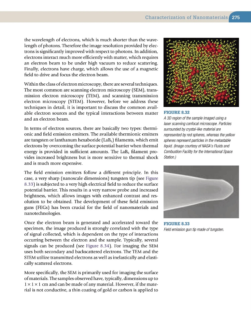
Figure 8.32
A 3D region of the sample imaged using a
laser scanning confocal microscope. Particles
surrounded by crystal-like material are
represented by red spheres, whereas the yellow
spheres represent particles in the metastable
liquid. (Image courtesy of NASA’s Fluids and
Combustion Facility for the International Space
Station.)
Figure 8.33
Field emission gun tip made of tungsten.
Characterization of Nanomaterials
the wavelength of electrons, which is much shorter than the wavelength of photons. Therefore the image resolution provided by electrons is significantly improved with respect to photons. In addition,
electrons interact much more efficiently with matter, which requires
an electron beam to be under high vacuum to reduce scattering.
Finally, electrons have charge, which allows the use of a magnetic
field to drive and focus the electron beam.
Within the class of electron microscopy, there are several techniques.
The most common are scanning electron microscopy (SEM), transmission electron microscopy (TEM), and scanning transmission
electron microscopy (STEM). However, before we address these
techniques in detail, it is important to discuss the common available electron sources and the typical interactions between matter
and an electron beam.
In terms of electron sources, there are basically two types: thermionic and field emission emitters. The available thermionic emitters
are tungsten or lanthanum hexaboride (LaB 6 ) filaments, which emit
electrons by overcoming the surface potential barrier when thermal
energy is provided in sufficient amounts. The LaB 6 filament provides increased brightness but is more sensitive to thermal shock
and is much more expensive.
The field emission emitters follow a different principle. In this
case, a very sharp (nanoscale dimensions) tungsten tip (see Figure
8.33) is subjected to a very high electrical field to reduce the surface
potential barrier. This results in a very narrow probe and increased
brightness, which allows images with enhanced contrast and resolution to be obtained. The development of these field emission
guns (FEGs) has been crucial for the field of nanomaterials and
nanotechnologies.
Once the electron beam is generated and accelerated toward the
specimen, the image produced is strongly correlated with the type
of signal collected, which is dependent on the type of interactions
occurring between the electron and the sample. Typically, several
signals can be produced (see Figure 8.34). For imaging the SEM
uses both secondary and backscattered electrons. The TEM and the
STEM utilize transmitted electrons as well as inelastically and elastically scattered electrons.
More specifically, the SEM is primarily used for imaging the surface
of materials. The samples observed have, typically, dimensions up to
1 × 1 × 1 cm and can be made of any material. However, if the material is not conductive, a thin coating of gold or carbon is applied to
Figure 8.32
A 3D region of the sample imaged using a
laser scanning confocal microscope. Particles
surrounded by crystal-like material are
represented by red spheres, whereas the yellow
spheres represent particles in the metastable
liquid. (Image courtesy of NASA’s Fluids and
Combustion Facility for the International Space
Station.)
Figure 8.33
Field emission gun tip made of tungsten.