

271
Soft lithographic methods are capable of producing nanostructures
in a wide range of materials and can print or mold on curved as well
as planar surfaces. They are not, however, ideal for nanoelectronics,
because circuits require stacked layers of different materials, and
distortion of soft PDMS stamps can produce errors in the patterns.
The large (and expanding) number of processes that manipulate
materials at the nanoscale are asssembled in the final synthesis
diagrams shown in Figure 8.27 and 8.28. Figure 8.27 summarizes
processes for making nanoclusters, nanolayers and nanofilms, as
well as methods for nanoprofiling to make nanoscale features.
Other processes are under development. Figure 8.28 summarizes
processes that are appropriate for different nanomaterial forms,
including nanoparticles, nanowires and nanotubes, nanofilms, and
bulk forms; and broadly suggests their relative scales. Figure 8.1
shown earlier summarizes processes according to the 0-D, 1-D, 2-D
and 3-D classification system discussed earlier.
8.2 characterization of
nanoMaterialS
In general, the role of characterization techniques is to establish a
correlation between the structure, shape, and chemical composition of nanomaterials obtained in processing, with their properties. In the case of nanomaterials, the important aspects to consider
about characterization methods are the type of information and
the resolution achieved by each technique. For each nanomaterial
Characterization of Nanomaterials
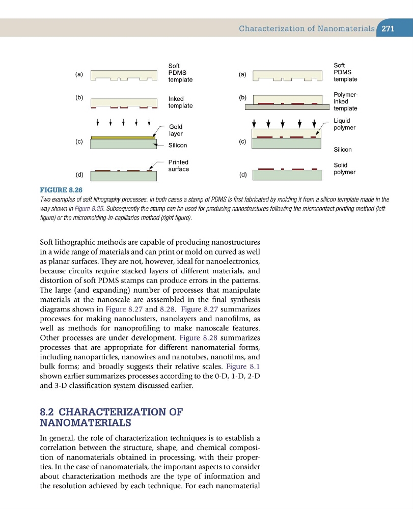
Figure 8.26
Two examples of soft lithography processes. In both cases a stamp of PDMS is first fabricated by molding it from a silicon template made in the
way shown in Figure 8.25. Subsequently the stamp can be used for producing nanostructures following the microcontact printing method (left
figure) or the micromolding-in-capillaries method (right figure).
Silicon
(b)
Inked
template
Gold
layer
(a)
Soft
PDMS
template
(c)
(d)
Printed
surface
Silicon
(b)
Polymerinked
template
Liquid
polymer
(a)
Soft
PDMS
template
(c)
(d)
Solid
polymer
Soft lithographic methods are capable of producing nanostructures
in a wide range of materials and can print or mold on curved as well
as planar surfaces. They are not, however, ideal for nanoelectronics,
because circuits require stacked layers of different materials, and
distortion of soft PDMS stamps can produce errors in the patterns.
The large (and expanding) number of processes that manipulate
materials at the nanoscale are asssembled in the final synthesis
diagrams shown in Figure 8.27 and 8.28. Figure 8.27 summarizes
processes for making nanoclusters, nanolayers and nanofilms, as
well as methods for nanoprofiling to make nanoscale features.
Other processes are under development. Figure 8.28 summarizes
processes that are appropriate for different nanomaterial forms,
including nanoparticles, nanowires and nanotubes, nanofilms, and
bulk forms; and broadly suggests their relative scales. Figure 8.1
shown earlier summarizes processes according to the 0-D, 1-D, 2-D
and 3-D classification system discussed earlier.
8.2 characterization of
nanoMaterialS
In general, the role of characterization techniques is to establish a
correlation between the structure, shape, and chemical composition of nanomaterials obtained in processing, with their properties. In the case of nanomaterials, the important aspects to consider
about characterization methods are the type of information and
the resolution achieved by each technique. For each nanomaterial
Characterization of Nanomaterials
Figure 8.26
Two examples of soft lithography processes. In both cases a stamp of PDMS is first fabricated by molding it from a silicon template made in the
way shown in Figure 8.25. Subsequently the stamp can be used for producing nanostructures following the microcontact printing method (left
figure) or the micromolding-in-capillaries method (right figure).
Silicon
(b)
Inked
template
Gold
layer
(a)
Soft
PDMS
template
(c)
(d)
Printed
surface
Silicon
(b)
Polymerinked
template
Liquid
polymer
(a)
Soft
PDMS
template
(c)
(d)
Solid
polymer