

chapter 8 nanomaterials: Synthesis and characterization
270
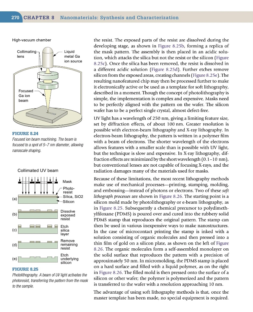
the resist. The exposed parts of the resist are dissolved during the
developing stage, as shown in Figure 8.25b, forming a replica of
the mask pattern. The assembly is then placed in an acidic solution, which attacks the silica but not the resist or the silicon (Figure
8.25c). Once the silica has been removed, the resist is dissolved in
a different acidic solution (Figure 8.25d). Further etches remove
silicon from the exposed areas, creating channels (Figure 8.25e). The
resulting nanofeatured chip may then be processed further to make
it electronically active or be used as a template for soft lithography,
described in a moment. Though the concept of photolithography is
simple, the implementation is complex and expensive. Masks need
to be perfectly aligned with the pattern on the wafer. The silicon
wafer has to be a perfect single crystal, almost defect-free.
UV light has a wavelength of 250 nm, giving a limiting feature size,
set by diffraction effects, of about 100 nm. Greater resolution is
possible with electron-beam lithography and X-ray lithography. In
electron-beam lithography, the pattern is written in a polymer film
with a beam of electrons. The shorter wavelength of the electrons
allows features with a smaller scale than is possible with UV light,
but the technique is slow and expensive. In X-ray lithography, diffraction effects are minimized by the short wavelength (0.1–10 nm),
but conventional lenses are not capable of focusing X-rays, and the
radiation damages many of the materials used for masks.
Because of these limitations, the most recent lithography methods
make use of mechanical processes—printing, stamping, molding,
and embossing—instead of photons or electrons. Two of these soft
lithograph processes are shown in Figure 8.26. The starting point is a
silicon mold made by photolithography or e-beam lithography, as
in Figure 8.25. Subsequently a chemical precursor to polydimethylfiloxane (PDMS) is poured over and cured into the rubbery solid
PDMS stamp that reproduces the original pattern. The stamp can
then be used in various inexpensive ways to make nanostructures.
In the case of microcontact printing the stamp is inked with a
solution consisting of organic molecules and then pressed into a
thin film of gold on a silicon plate, as shown on the left of Figure
8.26. The organic molecules form a self-assembled monolayer on
the solid surface that reproduces the pattern with a precision of
approximately 50 nm. In micromolding, the PDMS stamp is placed
on a hard surface and filled with a liquid polymer, as on the right
in Figure 8.26. The filled mold is then pressed onto the surface of a
silicon or other wafer; the polymer is polymerized and the pattern
is transferred to the wafer with a resolution approaching 10 nm.
The advantage of using soft lithography methods is that, once the
master template has been made, no special equipment is required.
Collimating
lens
Focused
Ga ion
beam
Liquid
metal Ga
ion source
High-vacuum chamber
Figure 8.24
Focused ion beam machining. The beam is
focused to a spot of 5–7 nm diameter, allowing
nanoscale shaping.
Figure 8.25
Photolithography. A beam of UV light activates the
photoresist, transferring the pattern from the mask
to the sample.
Silicon
Silica, SiO2
Collimated UV beam
Photoresist
Mask
(a)
(b)
(c)
(d)
(e)
Dissolve
exposed
resist
Etch
silica
layer
Remove
remaining
resist
Etch
underlying
silicon
270
the resist. The exposed parts of the resist are dissolved during the
developing stage, as shown in Figure 8.25b, forming a replica of
the mask pattern. The assembly is then placed in an acidic solution, which attacks the silica but not the resist or the silicon (Figure
8.25c). Once the silica has been removed, the resist is dissolved in
a different acidic solution (Figure 8.25d). Further etches remove
silicon from the exposed areas, creating channels (Figure 8.25e). The
resulting nanofeatured chip may then be processed further to make
it electronically active or be used as a template for soft lithography,
described in a moment. Though the concept of photolithography is
simple, the implementation is complex and expensive. Masks need
to be perfectly aligned with the pattern on the wafer. The silicon
wafer has to be a perfect single crystal, almost defect-free.
UV light has a wavelength of 250 nm, giving a limiting feature size,
set by diffraction effects, of about 100 nm. Greater resolution is
possible with electron-beam lithography and X-ray lithography. In
electron-beam lithography, the pattern is written in a polymer film
with a beam of electrons. The shorter wavelength of the electrons
allows features with a smaller scale than is possible with UV light,
but the technique is slow and expensive. In X-ray lithography, diffraction effects are minimized by the short wavelength (0.1–10 nm),
but conventional lenses are not capable of focusing X-rays, and the
radiation damages many of the materials used for masks.
Because of these limitations, the most recent lithography methods
make use of mechanical processes—printing, stamping, molding,
and embossing—instead of photons or electrons. Two of these soft
lithograph processes are shown in Figure 8.26. The starting point is a
silicon mold made by photolithography or e-beam lithography, as
in Figure 8.25. Subsequently a chemical precursor to polydimethylfiloxane (PDMS) is poured over and cured into the rubbery solid
PDMS stamp that reproduces the original pattern. The stamp can
then be used in various inexpensive ways to make nanostructures.
In the case of microcontact printing the stamp is inked with a
solution consisting of organic molecules and then pressed into a
thin film of gold on a silicon plate, as shown on the left of Figure
8.26. The organic molecules form a self-assembled monolayer on
the solid surface that reproduces the pattern with a precision of
approximately 50 nm. In micromolding, the PDMS stamp is placed
on a hard surface and filled with a liquid polymer, as on the right
in Figure 8.26. The filled mold is then pressed onto the surface of a
silicon or other wafer; the polymer is polymerized and the pattern
is transferred to the wafer with a resolution approaching 10 nm.
The advantage of using soft lithography methods is that, once the
master template has been made, no special equipment is required.
Collimating
lens
Focused
Ga ion
beam
Liquid
metal Ga
ion source
High-vacuum chamber
Figure 8.24
Focused ion beam machining. The beam is
focused to a spot of 5–7 nm diameter, allowing
nanoscale shaping.
Figure 8.25
Photolithography. A beam of UV light activates the
photoresist, transferring the pattern from the mask
to the sample.
Silicon
Silica, SiO2
Collimated UV beam
Photoresist
Mask
(a)
(b)
(c)
(d)
(e)
Dissolve
exposed
resist
Etch
silica
layer
Remove
remaining
resist
Etch
underlying
silicon